Metal oxide particles for bonding, sintering binder including same, process for producing metal oxide particles for bonding, and method for bonding electronic components

a technology of metal oxide particles and metal oxide particles, which is applied in the direction of transportation and packaging, solid-state devices, non-conductive materials with dispersed conductive materials, etc., can solve the problems of metal copper oxidizing into cuprous oxide, silver tends to undergo ionic migration, and short circui

Inactive Publication Date: 2017-09-28
HITACHI LTD
View PDF1 Cites 7 Cited by
  • Summary
  • Abstract
  • Description
  • Claims
  • Application Information

AI Technical Summary

Benefits of technology

[0016]The present invention can provide a sintering binder including copper-based particles, a method for producing the sintering binder, and a method for bonding using the sintering binder. The sintering binder mainly includes copper-cuprous oxide composite nanoparticles which combine stability and bondability and which less undergo the ionic migration.

Problems solved by technology

Disadvantageously, however, silver tends to undergo an ionic migration, and this often causes a short circuit.
Disadvantageously, however, the cleaning of the copper nanoparticles causes metal copper to be oxidized into cuprous oxide.

Method used


Image

  • Metal oxide particles for bonding, sintering binder including same, process for producing metal oxide particles for bonding, and method for bonding electronic components
  • Metal oxide particles for bonding, sintering binder including same, process for producing metal oxide particles for bonding, and method for bonding electronic components
  • Metal oxide particles for bonding, sintering binder including same, process for producing metal oxide particles for bonding, and method for bonding electronic components

Examples


example 1

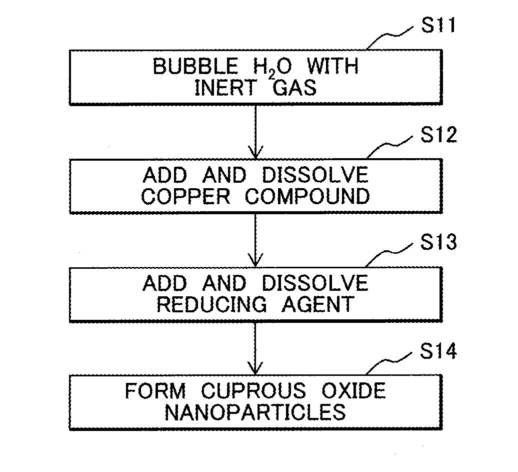
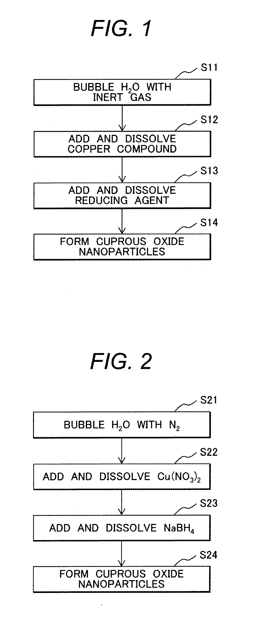
[0065]Preparation of Copper Oxide Nanoparticles

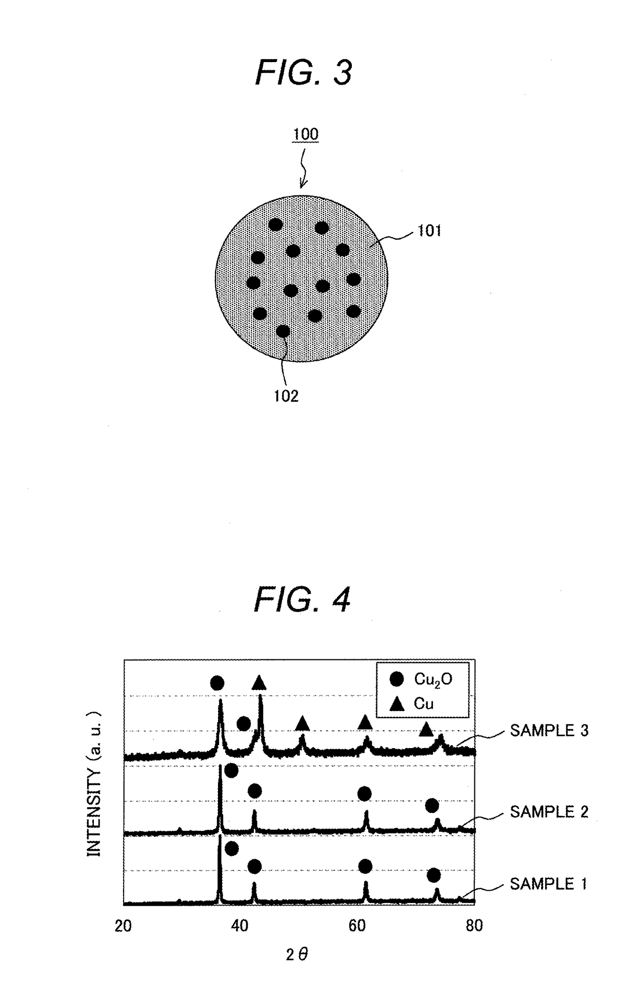
[0066]There were used Cu(NO3)2.3H2O powder (supplied by Kanto Chemical Co., Inc.) as a material copper compound; water as a solvent; and NaBH4 (supplied by Kanto Chemical Co., Inc., 92.0%) as a precipitating agent for copper-cuprous oxide nanoparticles. Distilled water was bubbled with nitrogen for 30 minutes in a 1000-mL capacity beaker, and 1000 mL of the distilled water after bubbling were combined with the Cu(NO3)2.3H2O powder so as to give a copper ion concentration of 0.01 mol / L, and the powder was uniformly dissolved on a water bath at 40° C. Thereafter 0.2 to 0.6 mol / mL NaBH4 aqueous solution (50 mL) was added dropwise, and synthetically yielded copper-cuprous oxide nanoparticles.

[0067]After stirring at room temperature for 24 hours, the synthesized copper-cuprous oxide nanoparticles were subjected to centrifugal separation and cleaning (washing) each three times using a centrifugal cleaner Suprema 21 (supplied by Tomy Seiko Co....

example 2

[0077]Bonding Strength Test of Copper-Cuprous Oxide Composite Nanoparticles

[0078]Bonding strength tests were performed while simulating bonding of electronic components with each other. The tests were performed each in the following manner. Copper test specimens used in the measurement were a lower test specimen having a diameter of 10 mm and a thickness of 5 mm; and an upper test specimen having a diameter of 5 mm and a thickness of 2 mm. The prepared sintering binder was applied onto the lower test specimen, and the upper test specimen was placed on the applied sintering binder, followed by a sintering heat treatment at a temperature of 400° C. in hydrogen for 5 minutes. This process was performed while a load in terms of compacting pressure of 1.2 MPa was applied. A shear stress was loaded on the test specimens after bonding at a rate of shear of 30 mm / min, and a peak load at rupture was measured using a shear tester (Bond Tester SS-100KP, supplied by Seishin Trading Co., Ltd., m...

example 3

[0082]Application to Semiconductor Devices

[0083]FIG. 6A is a plan view of an insulated semiconductor device to which the present invention is applied. FIG. 6B is a cross-sectional view taken along the line A-A in FIG. 6A. FIG. 7 is a perspective view of the principal part of the device in FIG. 6A. FIG. 8 is a schematic enlarged cross-sectional view of a portion where the semiconductor element illustrated in FIG. 6A is placed. The semiconductor device will be illustrated below with reference to FIGS. 6A, 6B, 7, and 8.

[0084]A circuit board including a ceramic insulated substrate 303 and an interconnection layer 302 is bonded through a solder layer 309 to a supporting substrate 310. The interconnection layer 302 includes copper interconnections coated with nickel. A collector electrode 307 of the semiconductor element 301 is bonded to the interconnection layer 302 on the ceramic insulated substrate 303 through a bonding layer 305 formed from the copper-cuprous oxide composite particles...


PUM

PropertyMeasurementUnit
particle sizeaaaaaaaaaa
sizeaaaaaaaaaa
sizeaaaaaaaaaa

Abstract

Provided are: a sintering binder including nanoparticles, a method for producing the sintering binder, and a method for bonding using the sintering binder. The sintering binder mainly includes cuprous oxide nanoparticles, combines particle stability with bondability, and less undergoes ion migration. A composite particle including metallic copper with the remainder being cuprous oxide and inevitable impurities is used for bonding typically of metals. The composite particle structurally includes metallic copper dispersed inside the particle and has an average particle size of 1000 nm or less.

Description

TECHNICAL FIELD[0001]The present invention relates to metal oxide particles for bonding, a sintering binder containing the metal oxide particles, a method for producing the metal oxide particles for bonding, and a method for bonding electronic components.BACKGROUND ART[0002]Metal nanoparticles (such as ones having a particle size of 100 nm or less) have large surface areas as compared to the volumes thereof, offer high chemical activities, and can be sintered at significantly lower temperatures. The metal nanoparticles therefore receive attention as novel functional materials. For example, pastes containing such metal nanoparticles are expected as materials for use in bonding of electronic components with each other, and formation of circuit wiring (circuit interconnections) in electronic devices. In these uses, generally preferred are metal nanoparticles having thermal conductivity, electroconductivity, and heat resistance (oxidation resistance) at high levels. These uses therefore...

Claims


Application Information

Patent Timeline
Patent Type & Authority Applications(United States)
IPC IPC(8): H01B1/22H01R4/02B82Y30/00C01G3/02H01L21/52B22F1/105
CPCH01B1/22C01G3/02H01R4/02B82Y30/00H01L21/52H01L2224/40225H01L2224/32225H01L2224/48227H01L2224/37599H01L2224/371H01L2224/37147C01P2002/72C01P2004/62C01P2004/80B22F3/1003B22F9/24C22C1/05H01L2224/73265H01L2924/19107B22F1/105H01L2224/73221H01L2924/00014H01L2924/00
Inventor YASUDA, YUSUKEMORITA, TOSHIAKIKOBAYASHI, YOSHIOMAEDA, TAKAFUMI
Owner HITACHI LTD
Why Eureka
Try Eureka