Semiconductor treatment composition and treatment method

a technology of semiconductors and compositions, applied in the direction of lapping machines, aqueous dispersions, polishing compositions, etc., can solve the problems of affecting the performance the surface of the polishing machine is easily contaminated with iron, and the device may fail to work properly, so as to reduce the damage applied, effectively remove the surface of the processing target, and effectively remove the polishing waste

Active Publication Date: 2017-11-16
JSR CORPORATIOON
View PDF1 Cites 3 Cited by
  • Summary
  • Abstract
  • Description
  • Claims
  • Application Information

AI Technical Summary

Benefits of technology

[0023]The semiconductor treatment composition according to one embodiment of the invention can reduce damage applied to a metal wire and the like included in the processing target, and can still effectively remove contaminants from the surface of the processing target.
[0024]The exemplary embodiments of the invention are described in detail below. Note that the invention is not limited to the exemplary embodiments described below. The invention includes various modifications that may be implemented without departing from the scope of the invention.
[0025]A semiconductor treatment composition according to one embodiment of the invention includes particles having a particle size of 0.1 to 0.3 micrometers in a number of 3×101 to 1.5×10³ per mL. The semiconductor treatment composition may be a concentrated-type semiconductor treatment composition that is used after being diluted with a liquid medium (e.g., purified water and organic solvent), or may be a non-dilution-type semiconductor treatment composition that is used without being diluted. The term “semiconductor treatment composition” used herein includes both the concentrated-type semiconductor treatment composition and the non-dilution-type semiconductor treatment composition unless otherwise specified.
[0026]The semiconductor treatment composition may be used as a treatment agent such as a cleaning agent for removing particles, metal impurities, and the like present on the surface of the treatment target (polishing target) after completion of CMP, a resist stripper for removing a resist from a semiconductor substrate that has been processed using a resist, and an etchant for shallowly etching the surface of a metal wire or the like to remove a surface contaminant. Note that the term “treatment agent” used herein includes a cleaning agent for cleaning a semiconductor surface, a resist stripper, an etchant, and the like. Each component included in the semiconductor treatment composition is described in detail below.
[0027]A semiconductor treatment composition according to one embodiment of the invention includes particles having a particle size of 0.1 to 0.3 micrometers (hereinafter may be referred to as “specific particles”) in a number of 3×101 to 1.5×10³ per mL. It is considered that, when the semiconductor treatment composition includes the specific particles in a number within a predetermined range, it is possible to effectively remove polishing waste that remains on the treatment target surface during the treatment step. If the semiconductor treatment composition includes the specific particles in a number more than the predetermined range, the specific particles may remain on the treatment target surface, and the electrical characteristics of the resulting semiconductor circuit (i.e., treatment target) may deteriorate, whereby a decrease in yield and the like may occur. If the semiconductor treatment composition includes the specific particles in a number less than the predetermined range, it may be difficult to effectively remove polishing waste that remains on the treatment target surface, and the flatness of the treatment target surface may deteriorate.
[0028]It is generally considered that a particle is foreign matter that should be removed as much as possible during a semiconductor device production process (see WO1999 / 049997, for example). However, it was found contrary to the above concept that it is possible to improve treatment performance without causing significant deterioration in semiconductor properties, by treating the treatment target surface by using a semiconductor treatment composition that includes particles having a particle size of 0.1 to 0.3 micrometers within a predetermined range.

Problems solved by technology

A fatal device defect may occur if such polishing waste remains.
Since an iron ion included in the CMP slurry is easily adsorbed on the surface of the polishing target, the polishing target surface is easily contaminated with iron.
In this case, however, the polished surface is easily etched and damaged.

Method used


Image

  • Semiconductor treatment composition and treatment method
  • Semiconductor treatment composition and treatment method
  • Semiconductor treatment composition and treatment method

Examples


example 1

4.1. Example 1

4.1.1. Preparation of Semiconductor Treatment Composition (Concentrated-Type Semiconductor Treatment Composition)

[0102]A polyethylene container was charged with each component listed in Table 1 in the ratio listed in Table 1. After the addition of a proper quantity of ion-exchanged water, the mixture was stirred for 15 minutes. Ion-exchanged water, potassium hydroxide, and sodium hydroxide were optionally added to the mixture so that the total amount of the components was 100 parts by mass to prepare a composition having the pH, the K content, and the Na content listed in Table 1.

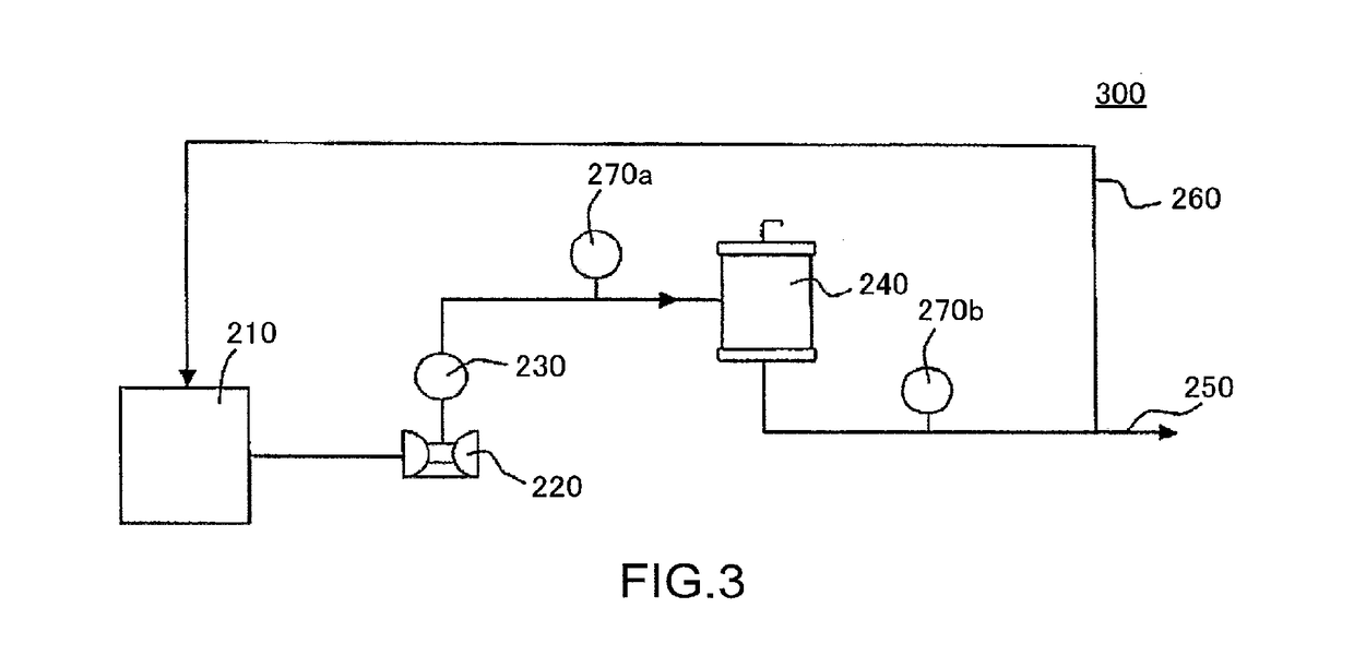
[0103]After the addition of 0.01 parts by mass of colloidal silica (“PL-1” manufactured by Fuso Chemical Co., Ltd., primary particle size: 15 nm) to 100 parts by mass of the composition, the mixture was filtered using the filtration device 300 illustrated in FIG. 3 (filtration step). The filtration device 300 illustrated in FIG. 3 includes a supply tank 210 that stores and supplies the composi...

example 27

4.3. Example 27

4.3.1. Preparation of Semiconductor Treatment Composition

[0145]A semiconductor treatment composition (concentrated-type semiconductor treatment composition) was prepared in the same manner as in Example 1, except that the composition was changed as listed in Table 3, and the pH, the K content, and the Na content were adjusted as listed in Table 3 using potassium hydroxide and sodium hydroxide, as required.

4.3.2. Wiring Board Cleaning Test

(1) Chemical Mechanical Polishing Step

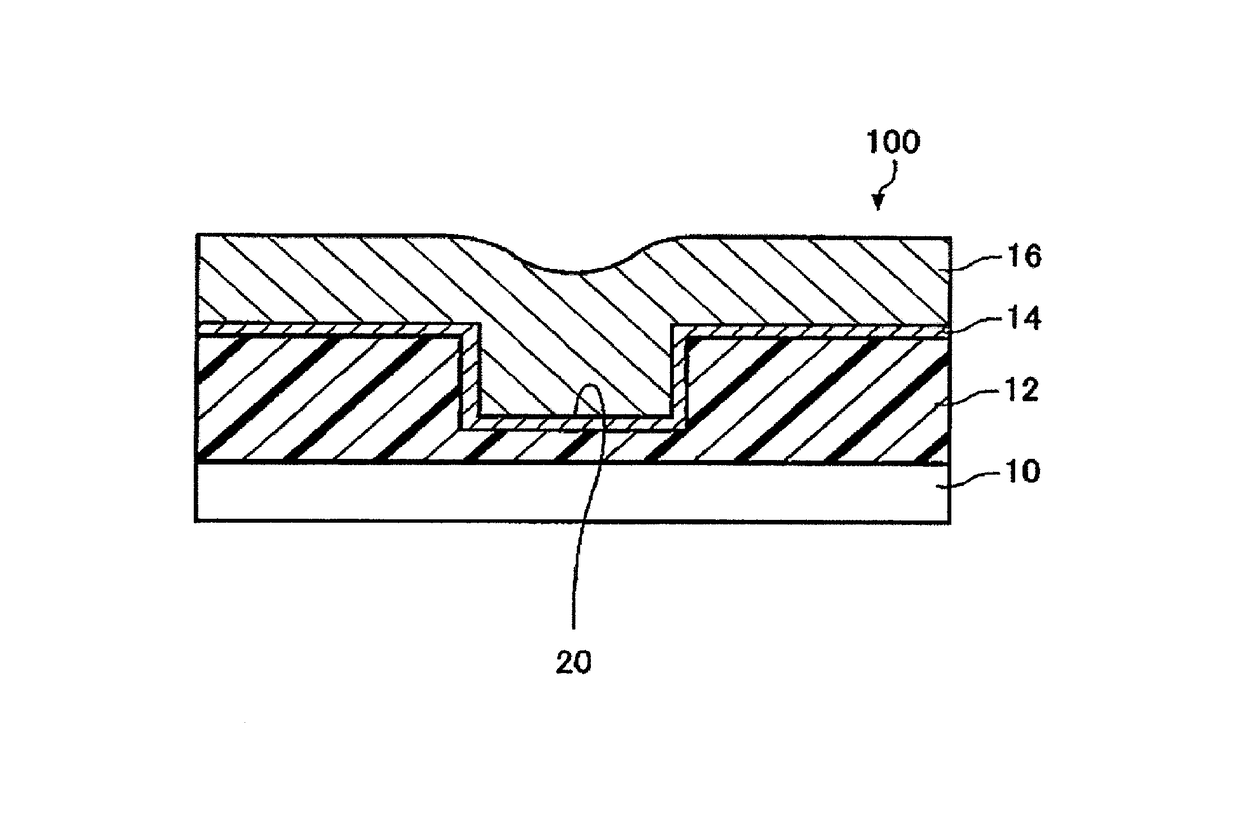
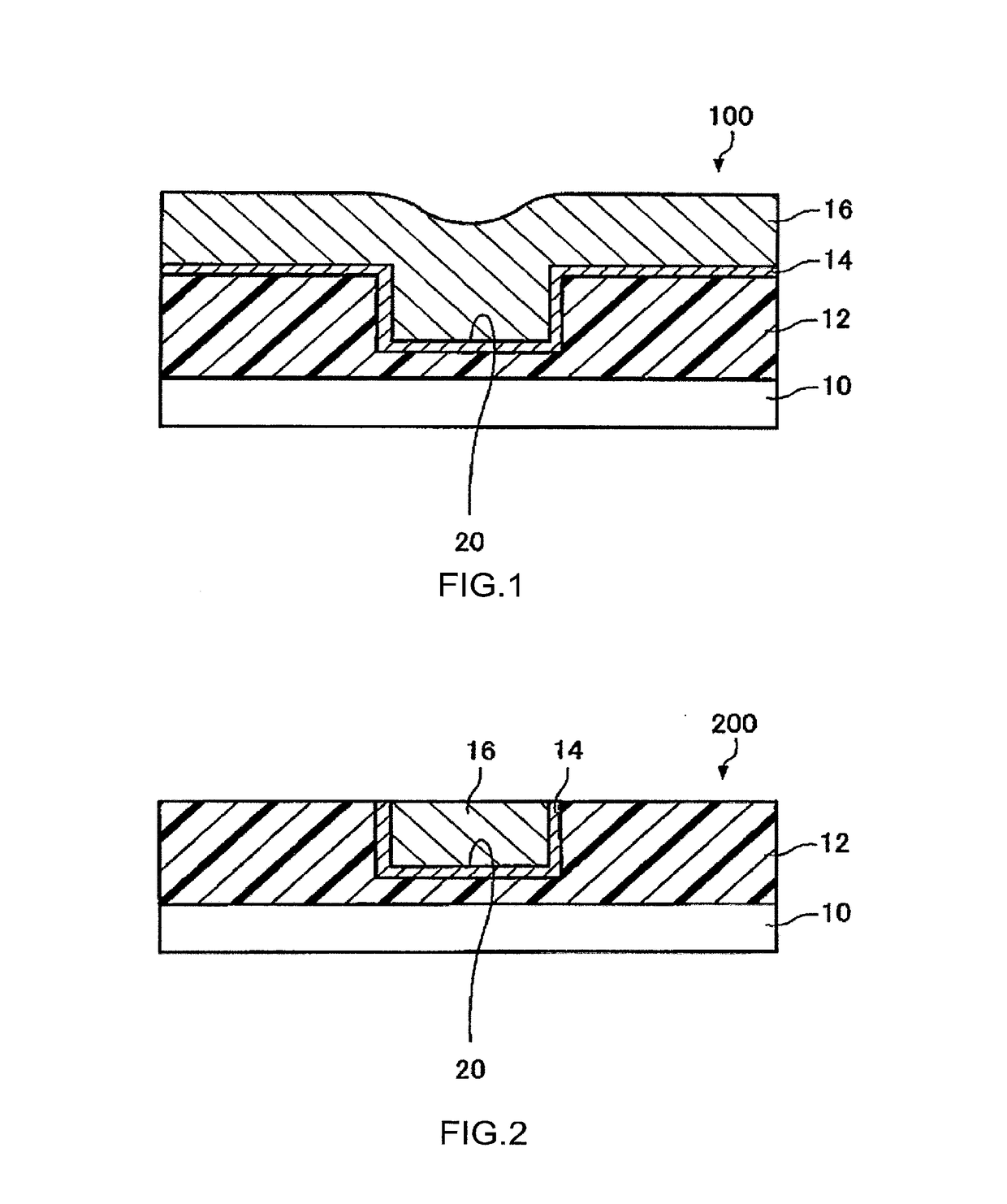
[0146]A substrate provided with a copper wire pattern (i.e., a test substrate obtained by stacking a PETEOS film on an 8-inch silicon substrate to a thickness of 5,000 angstroms, forming a pattern using a mask (“SEMATECH 854”), and sequentially stacking a cobalt film (thickness: 250 angstroms), a tungsten seed film (thickness: 1,000 angstroms), and a tungsten-plated film (thickness: 10,000 angstroms) thereon) was subjected to single-step chemical mechanical polishing under the following conditions...

examples 28 to 31

4.4. Examples 28 to 31 and Comparative Example 10

[0172]A semiconductor treatment composition (concentrated-type semiconductor treatment composition) was prepared in the same manner as in Example 27, except that the composition was changed as listed in Table 3, and a treatment agent (cleaning agent) was prepared in the same manner as in Example 27, except that the composition was changed as listed in Table 3. The wiring board treatment test and the evaluation tests were performed in the same manner as in Example 27.

4.5. Examples 32 to 35 and Comparative Examples 11 to 13

[0173]A polyethylene container was charged with each component listed in Table 4 in the ratio listed in Table 4, and the mixture was stirred for 15 minutes.

[0174]The resulting composition was filtered in the same manner as in Example 1, except that a filter in which a membrane-type cartridge filter “PE-CLEAN” (manufactured by Pall Corporation, nominal filtration rating: 0.05 micrometers, length: 10 inches) was provide...


PUM

PropertyMeasurementUnit
particle sizeaaaaaaaaaa
viscosityaaaaaaaaaa
particle sizeaaaaaaaaaa

Abstract

A semiconductor treatment composition includes particles having a particle size of 0.1 to 0.3 micrometers in a number of 3×101 to 1.5×10³ per mL.

Description

[0001]Japanese Patent Application No. 2016-094397 filed on May 10, 2016, Taiwanese Patent Application No. 105140526 filed on Dec. 8, 2016, Korean Patent Application No. 10-2017-0017333 filed on Feb. 8, 2017 and Chinese Patent Application No. 201710238028.2 filed on Apr. 12, 2017 are hereby incorporated by reference in their entirety.BACKGROUND OF THE INVENTION[0002]The present invention relates to a semiconductor treatment composition, and a treatment method that utilizes the semiconductor treatment composition.[0003]Chemical mechanical polishing (CMP) that is used to produce a semiconductor device is a technique that causes the processing target (polishing target) and a polishing pad to come in sliding contact with each other while pressing the processing target against the polishing pad, and supplying a chemical mechanical polishing aqueous dispersion (hereinafter may be referred to as “CMP slurry”) to the polishing pad to chemically and mechanically polish the processing target. ...

Claims


Application Information

Patent Timeline
Patent Type & Authority Applications(United States)
IPC IPC(8): H01L21/321H01L21/302H01L21/02H01L21/306H01L21/304
CPCH01L21/3212H01L21/30625H01L21/02052H01L21/304H01L21/02024H01L21/302B24B1/00B24B37/044C09G1/00C09G1/02C09G1/04C09G1/06C09K3/1454C09K3/1463C09K13/06C11D3/14C11D7/20C11D11/0047H01L21/02074
Inventor KAMEI, YASUTAKAHAYAMA, TAKAHIRONISHIGUCHI, NAOKIKAMO, SATOSHISHINODA, TOMOTAKA
Owner JSR CORPORATIOON
Why Eureka
Try Eureka