Optical semiconductor device, optical module, and method for manufacturing optical semiconductor device

Active Publication Date: 2018-03-29
LUMENTUM JAPAN INC
View PDF2 Cites 3 Cited by
  • Summary
  • Abstract
  • Description
  • Claims
  • Application Information

AI Technical Summary

Benefits of technology

[0019]The invention provides an optical semiconductor device, an optical module, and a method for manufacturing an optical semico

Problems solved by technology

Generally, in the ridge waveguide laser, since there is a diffusion current in a transverse direction in a semiconductor layer under a ridge stripe of the ridge waveguide laser, an effective active layer is broadened, and since a current is transversely diffused to further outside thereof, there is an ineffective c

Method used


Image

  • Optical semiconductor device, optical module, and method for manufacturing optical semiconductor device
  • Optical semiconductor device, optical module, and method for manufacturing optical semiconductor device
  • Optical semiconductor device, optical module, and method for manufacturing optical semiconductor device

Examples


Example

[First Embodiment]

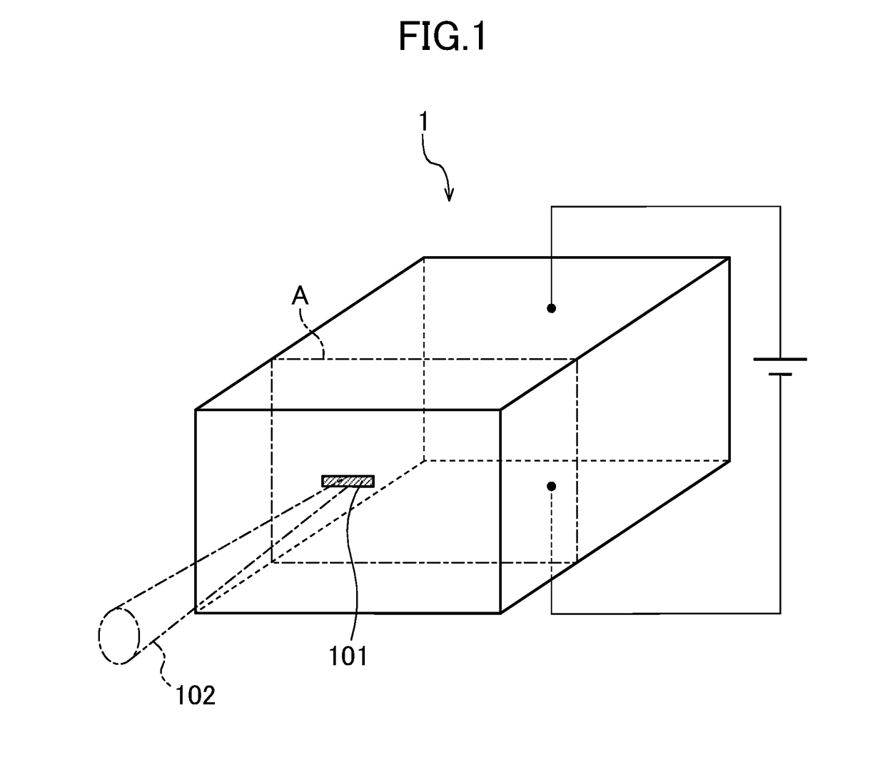
[0029]FIG. 1 is a diagram illustrating a schematic configuration of an optical semiconductor device 1 according to a first embodiment of the invention. The optical semiconductor device 1 illustrated in FIG. 1 is a semiconductor laser, and a voltage is applied to two electrodes disposed on opposite surfaces of a rectangular parallelepiped, thereby, laser light 102 is emitted from an oscillation region 101.

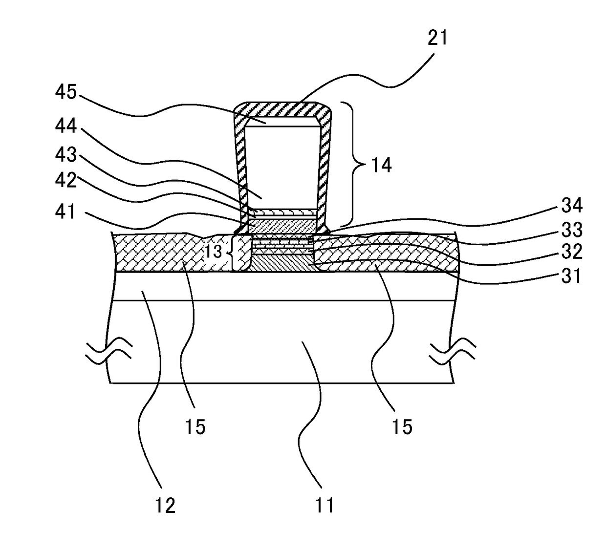
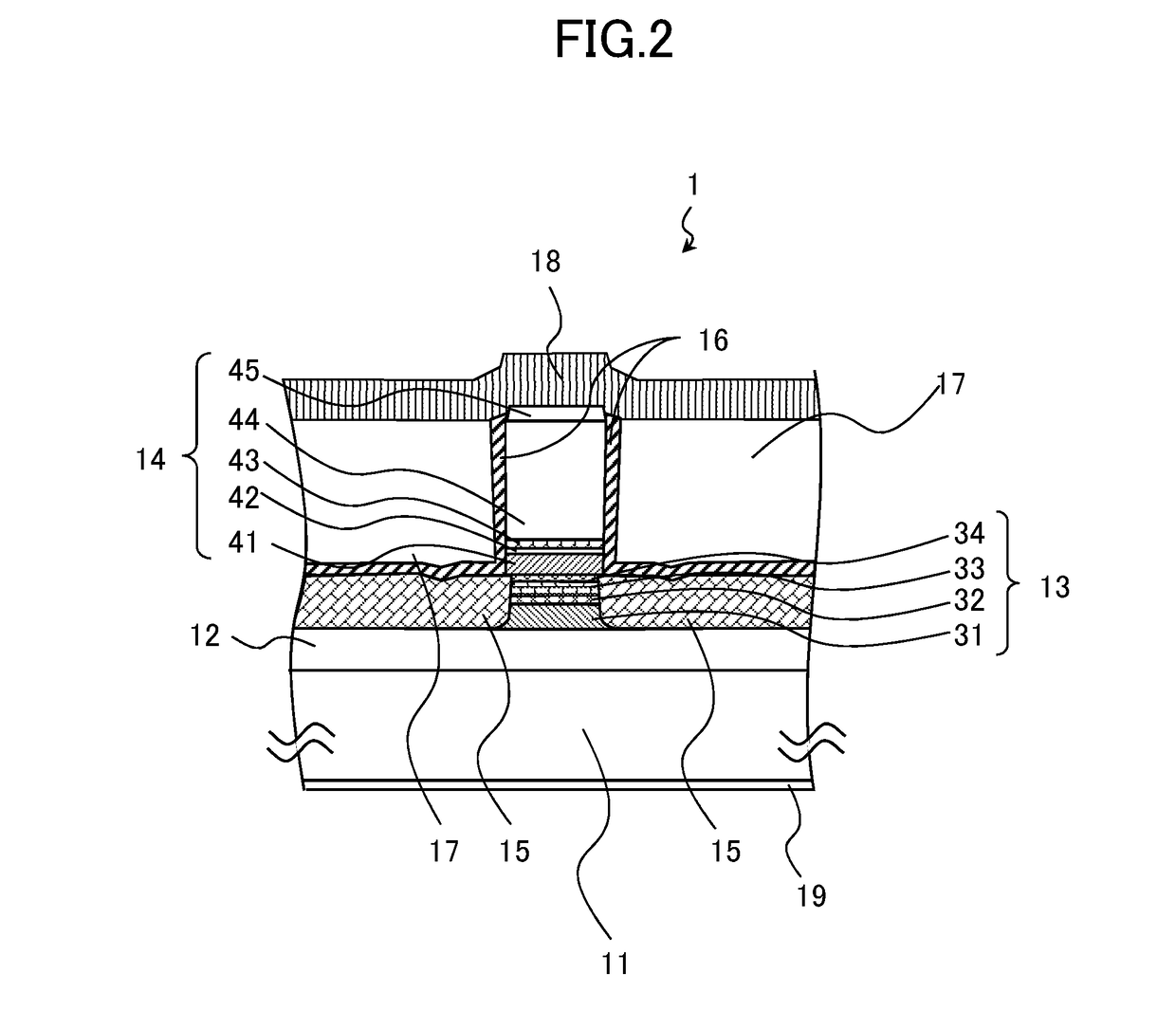
[0030]FIG. 2 is a sectional view in a cross section indicated by A of FIG. 1. FIG. 2 is a schematic diagram of the cross section perpendicular to an optical axis of a semiconductor laser which is oscillated in a 1.3 μm band of an optical fiber communication transmission light source. The optical semiconductor device 1 is configured to include a p type InP semiconductor substrate 11, a lower cladding layer 12, a lower mesa structure 13, an upper mesa structure 14, a buried semiconductor layer 15 that buries both side surfaces of the lower mesa structure 13, a first ...

Example

[Second Embodiment]

[0057]FIG. 5 is a sectional view of an optical semiconductor device 2 according to a second embodiment of the invention. FIG. 5 is a schematic diagram of the cross section perpendicular to the optical axis of the optical semiconductor device 2 which is oscillated in a 1.3 μm band of the optical fiber communication transmission light source. The optical semiconductor device 2 of the second embodiment is configured to include an n type InP semiconductor substrate 51, a lower cladding layer 52, a lower mesa structure 53, an upper mesa structure 54, a buried semiconductor layer 55 that buries both side surfaces of the lower mesa structure 53, a first insulating layer 56 that covers both side surfaces of the upper mesa structure 54 by being in contact with both side surfaces of the upper mesa structure 54, a second insulating layer 57 that covers the first insulating layer 56, a p type electrode 58 that is configured with Ti / Pt / Au, and an n type electrode 59 that uses ...

Example

[Third Embodiment]

[0069]FIG. 6 and FIG. 7 are sectional views of an optical semiconductor device 3 according to a third embodiment of the invention. FIG. 6 and FIG. 7 are schematic diagrams of the cross section perpendicular to the optical axis of the optical semiconductor device 3 which is oscillated in a 1.3 μm band of the optical fiber communication transmission light source. Since the optical semiconductor device 3 according to the third embodiment is the same as the optical semiconductor device 1 according to the first embodiment except that the configurations of an upper mesa structure 84 and a buried semiconductor layer 85 are different, repeated description will be omitted.

[0070]In the upper mesa structure 84 of the optical semiconductor device 3 according to the third embodiment, the positions of the n type InGaAsP-SCH layer 41 and the InGaAsP diffraction grating layer 43 are reversed in comparison with the first embodiment. Specifically, in the upper mesa structure 84 of t...


PUM


Abstract

Provided is an optical semiconductor device which has long-term reliability since a threshold current is small, and a relaxation oscillation frequency is high. An optical semiconductor device includes an InP semiconductor substrate, a lower mesa structure that is disposed above the InP semiconductor substrate, and includes a multiple quantum well layer, an upper mesa structure that is disposed on the lower mesa structure, and includes a cladding layer, a buried semiconductor layer that buries both side surfaces of the lower mesa structure, and an insulating film that covers both side surfaces of the upper mesa structure by being in contact with both side surfaces of the upper mesa structure, in which the lower mesa structure includes a first semiconductor layer, above the multiple quantum well layer, and the upper mesa structure includes a second semiconductor layer which is different from the cladding layer in composition, below the cladding layer.

Description

CROSS-REFERENCE TO RELATED APPLICATION[0001]The present application claims priority from Japanese application JP 2016-187517, filed on Sep. 26, 2016, the content of which is hereby incorporated by reference into this application.BACKGROUND OF THE INVENTION1. Field of the Invention[0002]The present invention relates to an optical semiconductor device, an optical module, and a method for manufacturing an optical semiconductor device.2. Description of the Related Art[0003]The Internet is established as an infrastructure that is indispensable to modern society from business to home life, and an application range thereof is widened such that the application range is from data processing for business to a portal site, or from a blog to Internet mail order sales, video, e-book or social networking service (SNS). In most cases of Internet communication, used is optical communication that is advantageous for high capacity and long distance through a high-speed router apparatus. Furthermore, ...

Claims


Application Information

Patent Timeline
IPC IPC(8): H01S5/227H01S5/343H01S5/24H01S5/12
CPCH01S5/227H01S5/343H01S5/24H01S5/02288H01S5/0287H01S5/12H01S5/2009H01S5/2214H01S5/2226H01S5/2275H01S5/34306H01S5/222H01S5/2224H01S2301/166H01S5/3213H01S5/02251G02B6/42H01S5/02253
Inventor NAKAHARA, KOUJIKITATANI, TAKESHI
Owner LUMENTUM JAPAN INC
Why Eureka
Try Eureka