Method for Producing Group III Nitride Semiconductor, Seed Substrate and Group III Nitride Semiconductor Crystal

a technology of nitride and semiconductor, which is applied in the direction of polycrystalline material growth, crystal growth process, chemically reactive gas, etc., can solve the problems of large dislocation density difference, low peeling property, and easy cracking of gan crystal growth, so as to improve peeling property and improve peeling property , the effect of improving the peeling property

Active Publication Date: 2018-04-05
TOYODA GOSEI CO LTD
View PDF5 Cites 2 Cited by
  • Summary
  • Abstract
  • Description
  • Claims
  • Application Information

AI Technical Summary

Benefits of technology

[0014]In the above method for producing a seed substrate, in the second step, the trench may be formed even on the surface of the base substrate until the base substrate is etched. In the third step, a hollow may remain between the base substrate and the low dislocation density region by preventing the trench formed on the base substrate from being filled with the low dislocation density region. Thereby, peeling property between the seed substrate and the object layer of the Group III nitride semiconductor grown through the flux method can be improved. The step (trench) may be formed over the whole periphery of the base substrate until the base substrate is etched.
[0015]In the present invention, the high dislocation density region is melted back at an initial stage of crystal growth of an object layer comprising a Group III nitride semiconductor through a flux method, and thereafter, the object layer is formed so as to cover holes formed due to melting back on the top surface of the low dislocation density region, and to remain cavities between the object layer and the high dislocation density region. This can further improve peeling property between the seed substrate and the object layer of grown Group III nitride semiconductor crystal.
[0016]The average dislocation density of the base layer is preferably 5×10⁸ / cm2 or less. The dislocation density of the object layer of grown Group III nitride semiconductor crystal can be reduced, and warpage also can be further reduced.
[0017]The present invention is preferable when a seed substrate having a diameter of two inches or more is employed. The larger the diameter of the seed substrate, the larger the warpage of the grown Group III nitride semiconductor crystal. However, according to the present invention, even when the seed substrate having a diameter of two inches or more is employed, warpage can be effectively reduced. It is particularly preferable when a seed substrate having a diameter of three inches or more is employed.
[0018]According to the present invention, peeling property between the seed substrate and the object layer of grown Group III nitride semiconductor crystal is improved, thereby a large-area Group III nitride semiconductor crystal wafer having no fracture or crack can be obtained with a high yield. The dislocation density of the wafer of Group III nitride semiconductor crystal can be reduced. Warpage of the wafer of Group III nitride semiconductor crystal can be reduced. Therefore, the wafer of Group III nitride semiconductor crystal is easy to grind, and a high quality Group III nitride semiconductor wafer with a narrow off-angle distribution and a low dislocation density can be produced.

Problems solved by technology

Since there is a difference in the linear expansion coefficients of the base substrate and the GaN crystal, fracture or crack may easily occur in the GaN crystal grown during cooling after the growth is finished.
However, in the flux method, the dislocation density is drastically decreased at an initial stage of growth so that the dislocation density difference is large along the thickness direction.
Therefore, large warpage occurs in the peeled GaN crystal.
Warpage causes a problem particularly when a large-area substrate is employed, and mass productivity is reduced.
WO 2012 / 128375, there was a problem that the quality of the GaN crystal is easily deteriorated.
That is, it was difficult to achieve both high quality and peeling property of the GaN crystal.

Method used


Image

  • Method for Producing Group III Nitride Semiconductor, Seed Substrate and Group III Nitride Semiconductor Crystal
  • Method for Producing Group III Nitride Semiconductor, Seed Substrate and Group III Nitride Semiconductor Crystal
  • Method for Producing Group III Nitride Semiconductor, Seed Substrate and Group III Nitride Semiconductor Crystal

Examples


embodiment 1

[0090]The method for producing a GaN according to Embodiment 1 will be described. Firstly, a seed substrate 100 was produced as follows.

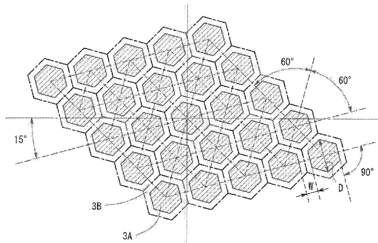
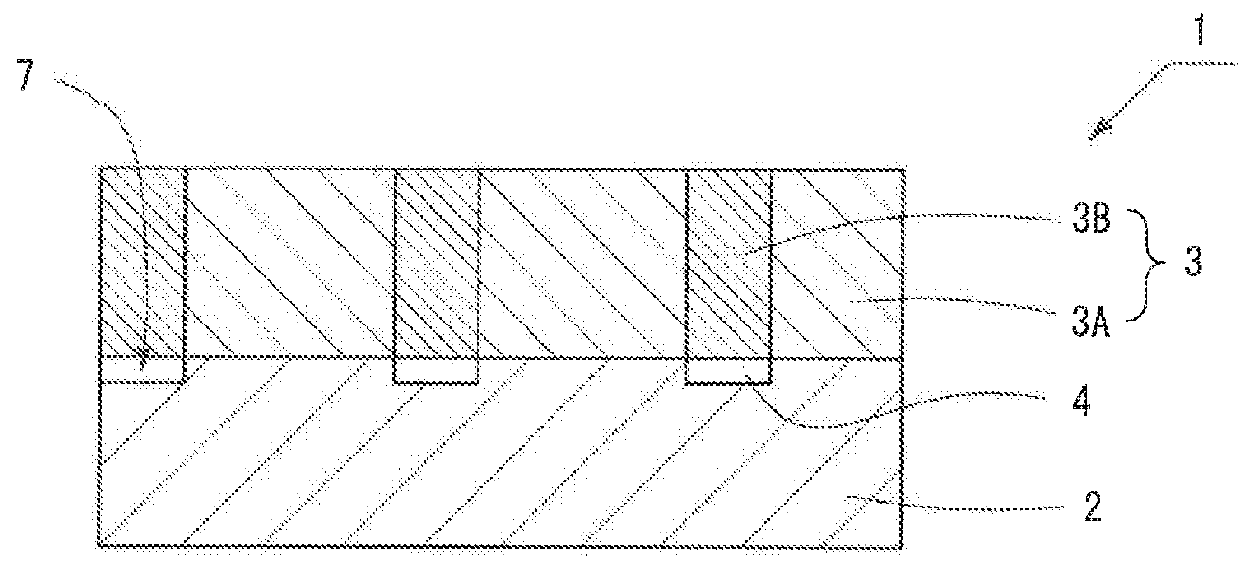
[0091]As shown in FIG. 6A, a template was prepared, in which a GaN layer 103 having a thickness of 5 μm was deposited on a base substrate 102 made of sapphire having a diameter of two inches and a thickness of 1 mm. On the GaN layer 103 of the template, a mask made of SiO2 having a prescribed pattern was formed. The mask was patterned through photolithography and RIE. The mask pattern was a regular hexagonal honeycomb pattern, and the interval between the opposite sides of each regular hexagon was 5 μm, and the interval between the adjacent regular hexagons was 2 μm (W of FIG. 2). The GaN layer 103 was etched through ICP until the base substrate 102 is etched by 0.1 mm to 0.3 mm, to form a trench 107 (refer to FIG. 6A). At this time, the mask was all etched, and the GaN layer 103 below the mask was etched up to 3.5 μm.

[0092]Subsequently, a GaN layer...

embodiment 2

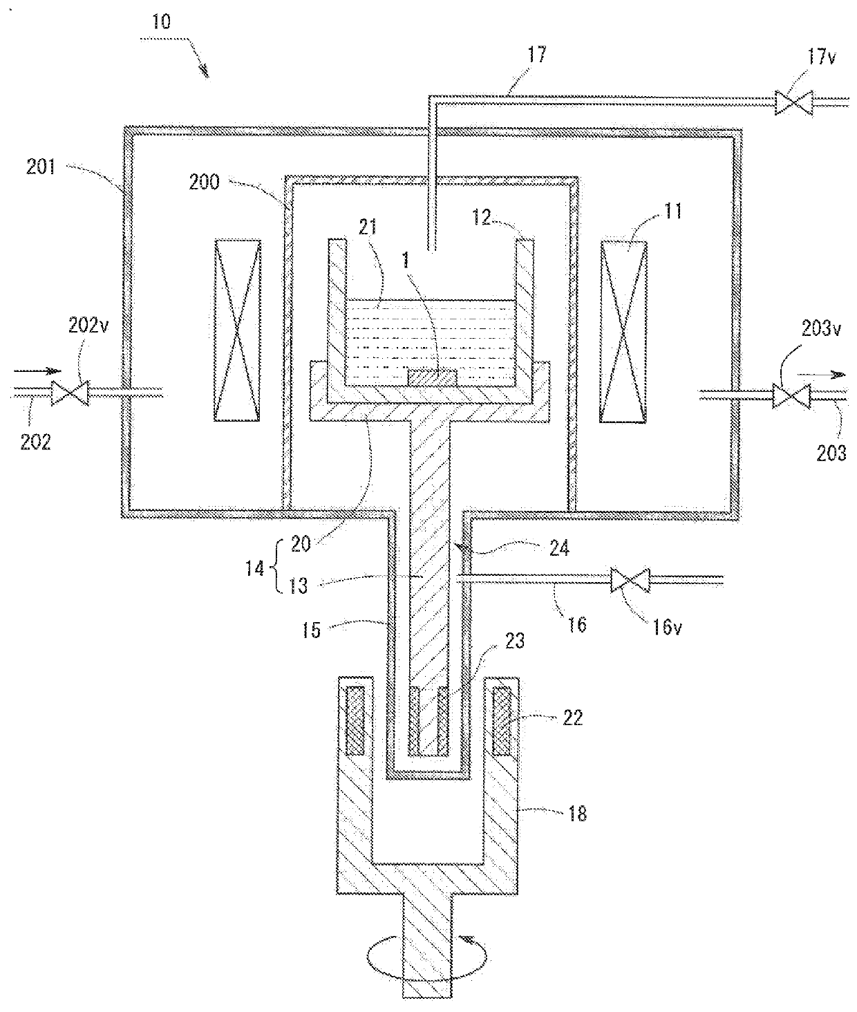
[0101]In Embodiment 1, the diameter of the seed substrate 100 was two inches, and the GaN crystal 106 was grown through a flux method for 40 hours so as to have a thickness of 0.6 mm in FIG. 7A. In Embodiment 2, the diameter of the seed substrate 100 was three inches, and the GaN crystal 106 was grown through a flux method for 160 hours so as to have three types of thicknesses of 0.9 mm, 1.1 mm, and 1.3 mm.

[0102]Three crucibles 12 were prepared. The Ga mole ratio of each crucible 12 was 18 mol %, 22 mol %, and 25 mol %, respectively. The liquid level was 7 mm in all crucibles. The growth conditions such as pressure and temperature were the same as in Embodiment 1. The growth time was 160 hours. In each crucible 12, the GaN crystal 106 grown on the seed substrate 100 had a thickness of 0.9 mm, 1.1 mm, and 1.3 mm, respectively. After the temperature was cooled down to room temperature, the GaN crystal 106 and the seed substrate were taken out from each crucible. The flat GaN crystal 1...


PUM

PropertyMeasurementUnit
diameteraaaaaaaaaa
widthaaaaaaaaaa
diameteraaaaaaaaaa

Abstract

The seed substrate comprises a base substrate and a base layer comprising a Group III nitride semiconductor formed on the base substrate, which has a high dislocation density region and a low dislocation density region. The planar pattern of the high dislocation density region is a honeycomb pattern. A hollow exists between the base substrate and the low dislocation density region. The object layer is grown through a flux method using the seed substrate. The high dislocation density region is melted back at an initial stage of crystal growth, and thereafter, the object layer is grown on the top surface of the low dislocation density region. A cavity remains between the high dislocation density region and the object layer. The presence of the cavity and the hollow makes easy to peel the object layer from the seed substrate.

Description

BACKGROUND OF THE INVENTIONField of the Invention[0001]The present invention relates to a method for producing a Group III nitride semiconductor through a flux method. The present invention also relates to a seed substrate employed for growing a Group III nitride semiconductor through a flux method.Background Art[0002]As a method for growing a Group III nitride semiconductor crystal, a flux method is known, in which nitrogen is dissolved in a molten mixture of alkali metal and Group III element such as Ga, and a Group III nitride semiconductor is epitaxially grown in liquid phase. A flux method in which Na (sodium) is generally used as alkali metal, is referred to as the Na flux method.[0003]In the Na flux method, a seed substrate (template substrate) having a GaN layer grown through MOCVD or a similar technique on a base substrate made of sapphire or a similar material is employed, and GaN is grown on the seed substrate. Since there is a difference in the linear expansion coefficie...

Claims


Application Information

Patent Timeline
Patent Type & Authority Applications(United States)
IPC IPC(8): H01L31/18C30B29/40C30B19/02C30B19/12C30B9/12
CPCH01L31/1856C30B29/406C30B19/02C30B19/12C30B9/12C30B9/06C30B9/10C30B19/00C30B25/02C30B25/18Y02E10/544
Inventor MORIYAMA, MIKIYAMAZAKI, SHIROKUMEGAWA, SHOHEI
Owner TOYODA GOSEI CO LTD
Why Eureka
Try Eureka