Power module with lead component and manufacturing method thereof

Active Publication Date: 2018-05-03
DELTA ELECTRONICS INC
View PDF12 Cites 16 Cited by
  • Summary
  • Abstract
  • Description
  • Claims
  • Application Information

AI Technical Summary

Benefits of technology

[0007]An object of the present invention is to provide a power module having a lead component and a manufacturing method thereof. The lead component is disposed on the carrier board, and the magnetic component and electronic device are vertically stacked relative to the lead component so as to accomplish a high-density integration of the power module and reduce the foot

Problems solved by technology

However, the circuit topology of the switching power supply is complex, so that the integrated density can't be effectively improved.
However, the leading terminal of the leadframe can only be led out at the edge of the printed circuit board and the printed circuit board should have a trace for further conduction, so as to increase the trace load on the printed circuit board and the power loss.
Furthermore, the leading terminal of the leadframe tends to be led out from the outside of the final forming module, and the package footprint of the module is increased.
In addition, if the power module uses a leadframe to lead out the pin of the surface-mount technology (SMT), the final formation of the pin pad area is small, so that it is unfavourable to be applied by the customers and reduce the loss of solder joints.
On the other hand, after the forming process of the leadframe, the frame part will be cut off and the material is wasted.
Further due to the existence of the frame, the entire area of the leadframe is larger, and the cost is increased.
Although the leading terminals of the power module can be arranged at any po

Method used


Image

  • Power module with lead component and manufacturing method thereof
  • Power module with lead component and manufacturing method thereof
  • Power module with lead component and manufacturing method thereof

Examples


Embodiment Construction

[0034]The present invention will now be described more specifically with reference to the following embodiments. It is to be noted that the following descriptions of preferred embodiments of this invention are presented herein for purpose of illustration and description only. It is not intended to be exhaustive or to be limited to the precise form disclosed.

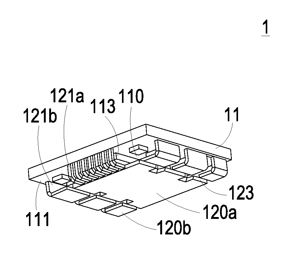
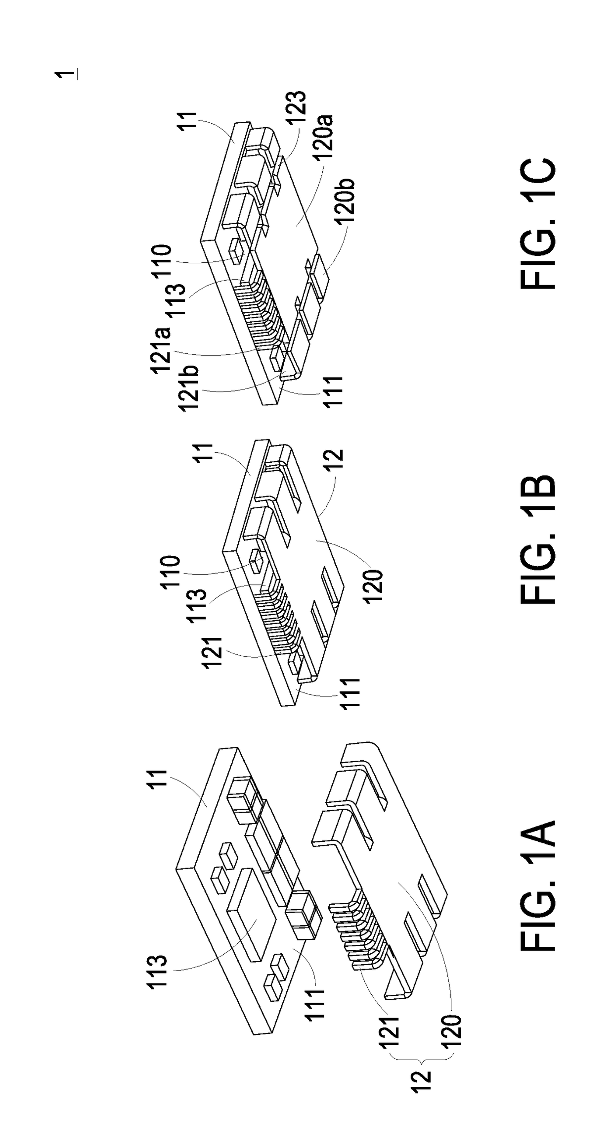
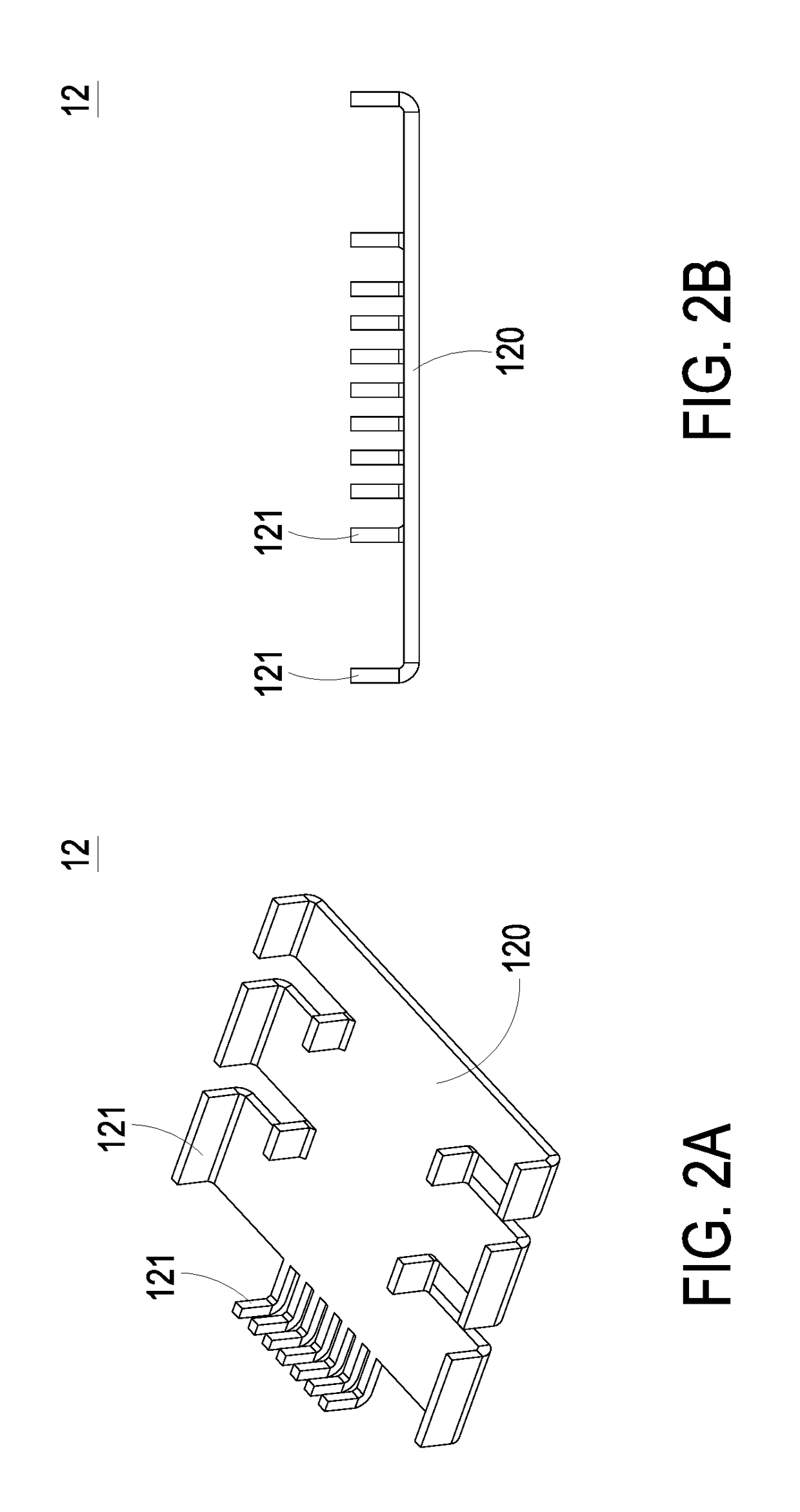
[0035]FIGS. 1A to 1C are schematic views illustrating an assembling flow of a power module according to a first preferred embodiment of the present invention. FIGS. 2A and 2B are a perspective view and a lateral view respectively illustrating the lead component of FIG. 1A. FIG. 3 is a flow chart showing a manufacturing method of a power module according to a first preferred embodiment of the present invention. As shown in FIGS. 1A to 1C, the power module 1 includes a carrier board 11 and at least one first lead component 12. The manufacturing method includes the following steps described in detail. Firstly, as shown in step S11 o...


PUM


Abstract

The present invention provides a power module and a manufacturing method thereof. The power module includes a carrier board and a lead component stacked relative to the carrier board. The lead component includes an initial plane, plural first pins and plural second pin. The initial plane includes a vertical projection overlapping with the carrier board. The first pins are electrically connected to the carrier board and vertical to the initial plane. The second pins are electrically connected to the carrier board and vertical to the initial plane. An isolation gap is disposed in the initial plane and located between the first pins and the second pins. The initial plane is separated into a first plane and a second plane by the isolation gap, so as to electrically isolate the first pins and the second pins from each other.

Description

FIELD OF THE INVENTION[0001]The present invention relates to a power module, and more particularly to a power module having a lead component and a manufacturing method thereof.BACKGROUND OF THE INVENTION[0002]In the conventional art, a switching power supply is often used to solve the problem of low conversion efficiency of the power system. However, the circuit topology of the switching power supply is complex, so that the integrated density can't be effectively improved. In order to minimize size and improve efficiency and application flexibility, the conventional power module has a leadframe to lead out the pin. The leadframe is used as the carrier of the integrated circuit chip, and the electrical connection between the output terminal of the chip and the outer leading wire is implemented by wire bonding. Consequently, the small terminal of the semiconductor chip is converted into the large-size output pin for facilitating the power module to assemble onto electronic devices or ...

Claims


Application Information

Patent Timeline
IPC IPC(8): H05K1/18H05K1/02H05K1/11H05K3/30H05K3/40H01L23/28
CPCH01L21/561H01L23/492H01L23/49517H01L23/49575H01L21/565H01L23/4334H01L23/49811H05K1/0265H05K2201/10272H01L23/3121H05K1/02H05K1/11H05K1/18H05K3/30H05K3/40
Inventor JI, PENGKAIHONG, SHOUYUZHAO, ZHENQINGZENG, JIANHONG
Owner DELTA ELECTRONICS INC
Why Eureka
Try Eureka