Flash Light Illumination Method and Organic Electronic Device Elements Obtainable This Way

a technology of electronic devices and flash light, which is applied in the direction of photovoltaic energy generation, semiconductor devices, solid-state devices, etc., can solve the problems of incongruity with the electronics industry, high cost and time consumption of methods, and the cost of device performance, so as to avoid electrical cross-talk, not time-consuming, and inexpensive

Active Publication Date: 2018-06-14
NOVALED GMBH
View PDF0 Cites 1 Cited by
  • Summary
  • Abstract
  • Description
  • Claims
  • Application Information

AI Technical Summary

Benefits of technology

[0007]Therefore, it is, in light of the prior art, the object of the present invention to provide a method for preparing an organic electronic device as well as respective organic electronic devices which may be constituted of an array of neighboring circuits or device elements overcoming drawbacks of the prior art. In particular, a method for preparing an organic electronic device shall be provided for avoiding electrical cross-talk between neighboring electrode areas comprised in the organic electronic device. The method shall be inexpensive, not time-consuming and suitable to obtain excellent device performance.

Problems solved by technology

These methods have the disadvantage of being expensive and time-consuming.
Reducing the thickness of the common conductive layers to a minimum of <10 nm can reduce the cross-talk phenomenon but is often at the expense of device performance.
However, this is contradicting the electronics industry's ambition for higher device density and resolution.
Especially for large area applications these techniques are too time-consuming.

Method used


Image

  • Flash Light Illumination Method and Organic Electronic Device Elements Obtainable This Way
  • Flash Light Illumination Method and Organic Electronic Device Elements Obtainable This Way
  • Flash Light Illumination Method and Organic Electronic Device Elements Obtainable This Way

Examples


Embodiment Construction

[0134]Following, the disclosure will be described in detail by referring to specific exemplary materials and conditions for performing the method by referring to the enclosed figures. In the figures show:

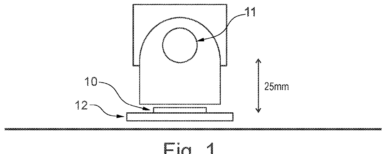
[0135]FIG. 1 Schematic view of the substrate with the layered structure placed under the fluid cooled Xenon flash lamp

[0136]FIG. 2 Test layout for measurements of the cross-talk current

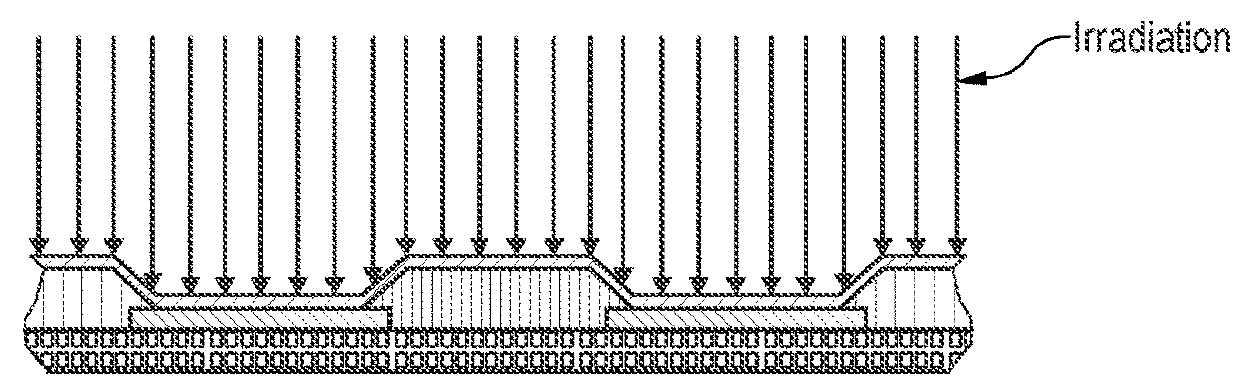
[0137]FIG. 3 Schematic cross-sectional view of the layered structure a) before irradiation, b) with irradiation, c) after irradiation.

[0138]FIG. 4 Resistance ratio of the redox-doped layer with and without grid

[0139]FIG. 5 Top view (large and detailed) of the grid on the substrate in a pixelated OLED layout

[0140]FIG. 6 Cross-talk current ratio before and after irradiation

[0141]FIG. 7 Optical density of grid vs first electrode

[0142]Table 1 Cross-talk currents on test layout for 40 μm channel at 5V

[0143]FIG. 1 shows a schematic view of the layered structure 10 being arranged below the source of the puls...


PUM

PropertyMeasurementUnit
conductivityaaaaaaaaaa
thicknessaaaaaaaaaa
thicknessaaaaaaaaaa

Abstract

The present invention relates to a method comprising the steps: a) providing a layered structure applicable for preparing an organic electronic device, comprising: aa) a substrate comprising a first electrode structure and a non-electrode part; bb) a grid formed by a grid material, wherein open areas of the grid are arranged above at least a part of the first electrode structure and the grid material is arranged above at least a part of the non-electrode part; and cc) a layer stack comprising at least one redox-doped layer having a conductivity of at least 1E−7 S/cm, the layer stack being deposited on the grid; wherein the optical density measured by absorption spectroscopy of the grid material is higher than the optical density of the open areas; and b) irradiating light pulses having a duration of <10 ms and an energy of 0.1 to 20 J/cm2 per pulse, alternatively 1 to 10 J/cm2, onto the layered structure; an organic electronic device obtainable this way and a device comprising said organic electronic device.

Description

[0001]The present invention relates to a method of using flash light illumination to prepare organic electronic devices.[0002]In electronics, crosstalk is a phenomenon by which a signal transmitted on one circuit or device creates an undesired effect in another circuit or device. Crosstalk is usually caused by undesired capacitive, inductive or conductive coupling from one circuit or device element, or part of a circuit or device element, to another. Electronic equipment having very low distances between circuits or device elements like high-resolution display screens, high resolution active matrix organic electronic diode (AMOLED) displays or thin-film transistor (TFT) arrays, photodetector arrays and image sensors the role of cross-talk is particularly prominent. The root cause is usually a conductive path between neighboring circuits or device elements brought about by common conductive layers or materials used in the device array.[0003]For example, common conductive layers may b...

Claims


Application Information

Patent Timeline
Patent Type & Authority Applications(United States)
IPC IPC(8): H01L51/56H01L27/32H01L51/00H01L51/52
CPCH01L51/56H01L27/3279H01L27/3246H01L27/322H01L51/0015H01L51/5243H10K71/60H10K50/805H10K71/00Y02E10/549H10K59/122H10K59/173H10K71/211H10K10/00H10K30/00H10K50/17H10K50/84H10K85/631H10K50/8423H10K59/38H10K59/1315
Inventor LANGGUTH, OLIVERCANZLER, TOBIAS
Owner NOVALED GMBH
Why Eureka
Try Eureka