Polymer-based, wideband electromagnetic wave shielding film

a wide-band electromagnetic wave and shielding film technology, applied in the direction of electrical equipment, conductors, conductive materials, etc., can solve the problems of electromagnetic waves emitted from electronic products, mutual interference between electronic products, stress, nervous system stimulation, etc., and achieve high shielding efficiency

Inactive Publication Date: 2018-07-19
KOREA ADVANCED INST OF SCI & TECH
View PDF2 Cites 18 Cited by
  • Summary
  • Abstract
  • Description
  • Claims
  • Application Information

AI Technical Summary

Benefits of technology

[0019]According to the present invention, a wideband electromagnetic wave shielding film based on a polymer may be provided by preparing a three-dimensional multilayer graphene-nanotube-metal oxide nanostructure in which a conductive material and a magnetic material are complexly combined, and then applying this nanostructure as a polymer filler. Accordingly, the present invention may provide a film which is flexible and has durability and high shielding efficiency, and thus, is suitable for being used as a shielding material in wearable electronics, flexible device and the like.

Problems solved by technology

Recently, as electromagnetic wave generation is increased due to rapid development and massive spread of computers, electronic products, communication devices and the like, a noise phenomenon due to electromagnetic waves in various frequency ranges is rapidly increased, thereby posing a problem that there occurs mutual interference between electronic products.
In addition, electromagnetic waves emitted from electronic products may cause stress, nervous system stimulation, heart diseases and the like in the human body.
Metal-based electromagnetic wave shielding materials show high electromagnetic wave shielding efficiency, but have a limitation in that it is heavy and corrosive to moisture.
Among these carbon-based shielding materials, graphene, carbon nanotubes and the like which are the 1-phase carbon-based materials were used, but had a limitation of low shielding efficiency.
As the 2-phase carbon-based materials, graphene / carbon nanotube composite materials, graphene-iron oxide composite materials and the like were used, but had problems such as a high filler content and low shielding efficiency.

Method used


Image

  • Polymer-based, wideband electromagnetic wave shielding film
  • Polymer-based, wideband electromagnetic wave shielding film
  • Polymer-based, wideband electromagnetic wave shielding film

Examples


preparation example 1

[0080]Synthesis of Graphene Oxide

[0081]First, a graphene oxide should be exfoliated from high-purity graphite, using a modified Hummer's method.

[0082]For this, 0.5 g of graphite (Samjung C&C, 99.95%, average size 200 μm) was added to 15 ml of sulfuric acid (H2SO4), and mixing was carried out by agitation at room temperature for 15 minutes.

[0083]Subsequently, 0.5 g of potassium permanganate (KMnO4) was slowly added to the mixed solution for 30 minutes. At that time, the solution was agitated in an ice bath.

[0084]Thereafter, the mixed solution was agitated in water at 50° C. for four hours.

[0085]Then, 150 ml of deionized water and 10 ml of hydrogen peroxide (H2O2) were added thereto and agitated for 30 minutes.

[0086]Further, a graphite oxide was neutralized by filtration, and a graphene oxide was exfoliated from the graphite oxide using a homogenizer.

[0087]Then, the graphene oxide was collected using a centrifuge and dried in an oven.

[0088]Synthesis of Multilayer Graphene-Nanotube-Met...

example 1

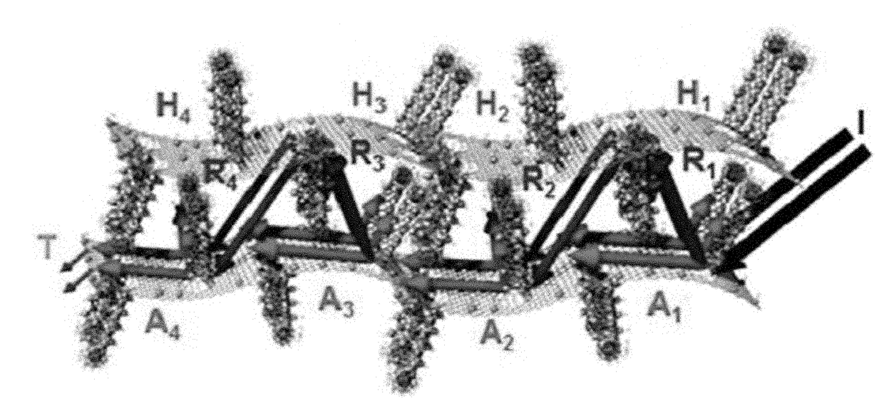
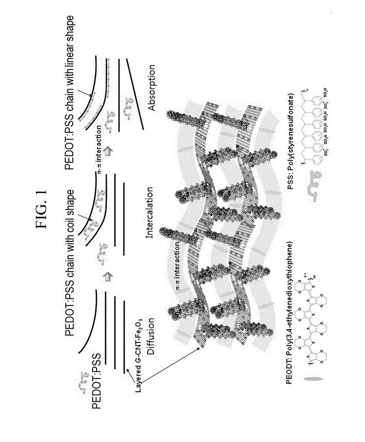
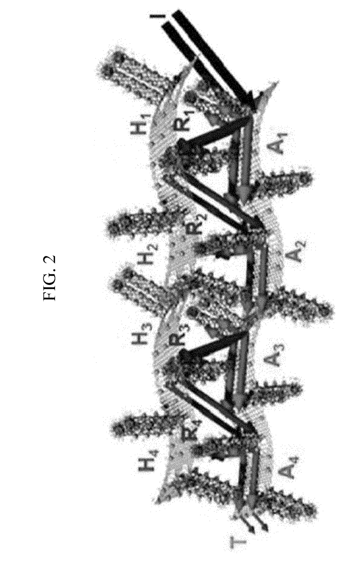
[0092]Manufacture of Polymer-Based Electromagnetic Wave Shielding Film Including Multilayer Graphene-Nanotube-Metal Oxide Nanostructure (Multilayered 3D G-CNT-Fe2O3)

[0093]PEDOT:PSS (poly(3,4-ethylenedioxythiophene) polystyrene sulfonate) and DMSO were mixed at a weight ratio of 98 / 2 to prepare a PEDOT:PSS water-soluble dispersion.

[0094]The multilayer graphene-nanotube-metal oxide nanostructure (3D G-CNT-Fe2O3) prepared in Preparation Example 1 and the PEDOT:PSS water-soluble dispersion were mixed at a weight ratio of 1:9, and then subjected to sonication for 30 minutes to be uniformly dispersed.

[0095]When dispersion was completed, the dispersion was poured to a petri dish, and dried (cured) in an oven at 40° C. for 12 hours, thereby obtaining a flexible electromagnetic wave shielding film.

experimental example 1

[0101]The photographs of the multilayer graphene-nanotube-metal oxide nanostructure (3D G-CNT-Fe2O3) of Preparation Example 1 were taken by a scanning electron microscope (SEM), and the result is shown in FIG. 4. In FIG. 4, a to i refer to images of identifying one nanostructure with multiple angles. That is, b and e are enlarged in a microscale, and the rest images are the results of identifying the detailed structure enlarged in a nanoscale.

[0102]In addition, the scanning electron microscope (SEM) photographs (a,b,c,d) and the high-resolution transmission electron microscope (TEM) photographs (e,f) of the multilayer graphene-nanotube-metal oxide nanostructure (3D G-CNT-Fe2O3) were taken and the result is shown in FIG. 5 by comparison. FIG. 5 is enlarged drawings of FIG. 4, in which a and b are drawings for identifying the multi-layer of the multilayer graphene-nanotube-metal oxide nanostructure, c is a drawing for identifying that nanotubes synthesized in a long shape are tangled ...


PUM

PropertyMeasurementUnit
weight ratioaaaaaaaaaa
thicknessaaaaaaaaaa

Abstract

The present invention relates to a polymer-based, wideband electromagnetic wave shielding film. More particularly, the present invention relates to a polymer-based, wideband electromagnetic wave shielding film capable of improving electromagnetic wave shielding and absorption performance, by applying a multilayer graphene-nanotube-metal oxide nanostructure in which a conductive material and a magnetic material are complexly combined, as a filler of the polymer.

Description

TECHNICAL FIELD[0001]The present invention relates to a polymer-based, wideband electromagnetic wave shielding film using a multilayer graphene-nanotube-metal oxide nanostructure, and more particularly, to a wideband electromagnetic wave shielding film capable of improving electromagnetic wave shielding and absorption performance, by preparing a multilayer graphene-nanotube-metal oxide nanostructure in which a conductive material and a magnetic material are complexly combined through microwave irradiation, and then applying the nanostructure as a polymer filler.BACKGROUND ART[0002]Recently, as electromagnetic wave generation is increased due to rapid development and massive spread of computers, electronic products, communication devices and the like, a noise phenomenon due to electromagnetic waves in various frequency ranges is rapidly increased, thereby posing a problem that there occurs mutual interference between electronic products. In addition, electromagnetic waves emitted fro...

Claims


Application Information

Patent Timeline
Patent Type & Authority Applications(United States)
IPC IPC(8): H05K9/00H01B1/02
CPCH01B1/023H05K9/0083
Inventor OH, ILKWONLEE, SI HWA
Owner KOREA ADVANCED INST OF SCI & TECH
Why Eureka
Try Eureka