Method for vertical gate-last process

a technology of metal oxides and transistors, applied in the direction of semiconductor devices, electrical equipment, nanotechnology, etc., can solve the problems of high-precision doping control along the axial direction of the nanowire, which has proved insufficient and is very challenging

Active Publication Date: 2018-08-02
WERNERSSON LARS ERIK +4
View PDF3 Cites 3 Cited by
  • Summary
  • Abstract
  • Description
  • Claims
  • Application Information

AI Technical Summary

Benefits of technology

[0003]To address the issues mentioned above, a self-aligned, gate-last process is utilized, with the possibility for local reduction of the nanowire diameter in the gated region using digital etching, while allowing for intrinsic channel and doped contact regions. Furthermore, the process allows the fabrication of MOSFETs with varying gate lengths in parallel on the same sample.

Problems solved by technology

High-precision doping control along the axial direction of the nanowire has proven insufficient and very challenging.
Furthermore, ohmic contacts typically require a high temperature annealing process to achieve sufficient low specific contact resistivity, whereas the electrical and structural properties of the gate dielectric are sensitive to high temperature processes.

Method used


Image

  • Method for vertical gate-last process
  • Method for vertical gate-last process
  • Method for vertical gate-last process

Examples


first embodiment

[0021]In the present invention, the upper ohmic transistor electrode is formed prior to the gate formation.

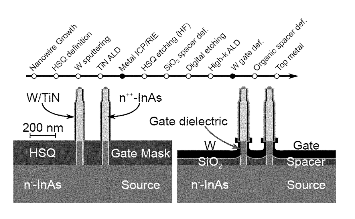
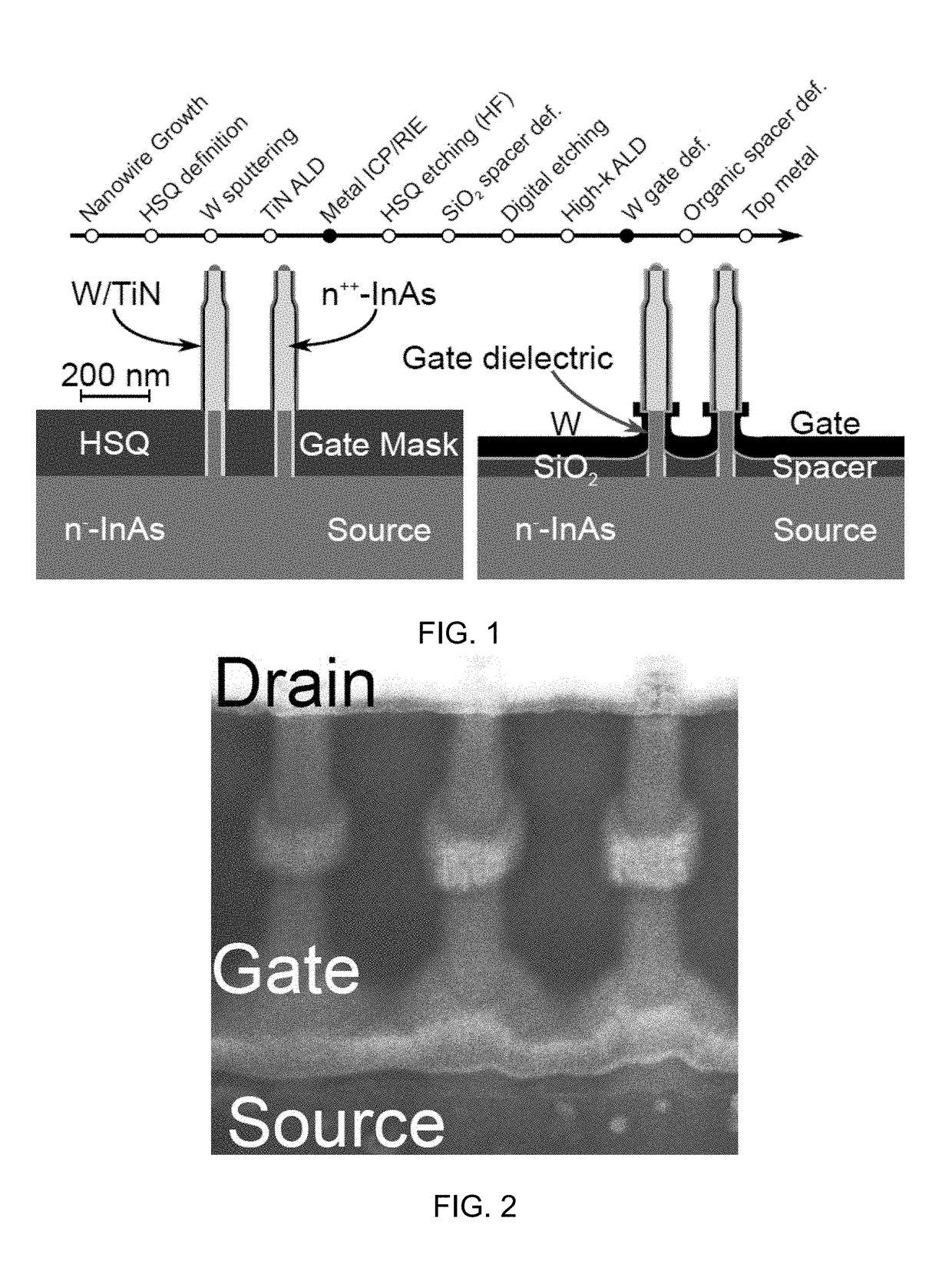
[0022]In a first step, the bottom of the nanowires is protected by one or several organic or inorganic layers, such as Hydrogen silsesquioxane (HSQ), SiNx, SiO2, BCB, photoresists. To achieve gate length control, the layer thickness is controlled around each nanowire, for instance via the control of the exposure dose or by local thinning of the layer by etching or by local addition of material by deposition. A top metal contact is formed by metal deposition, such as sputtering of 20 nm W and atomic layer deposition (ALD) of 5 nm TiN, or deposition of Ni. This metal is etched anisotropically for instance by dry etching, removing the planar layer and only keeping the metal on the nanowire sidewalls. The protection layer is then removed.

[0023]In a second step, an organic or inorganic spacer layer, such as SiO2, is deposited where the thickness of this layer is thinner than the fir...

second embodiment

[0027]In a second embodiment, the upper ohmic transistor electrode is formed prior to the gate formation.

[0028]In a first step, an ohmic contact is deposited below the gate region of the transistors.

[0029]In a second step, the region above the bottom ohmic contact is protected by an organic or inorganic layer, such as Hydrogen silsesquioxane (HSQ), SiNx, SiO2, BCB, photoresists. To achieve gate length control, the layer thickness is controlled around each nanowire, for instance via the control of the exposure dose or by local thinning of the layer by etching or by local addition of material by deposition. A top metal contact is formed by metal deposition, such as by sputtering of 20 nm W and atomic layer deposition (ALD) of 5 nm TiN or deposition of Ni. This metal is etched anisotropically for instance by dry etching, removing the planar layer and only keeping the metal on the nanowire sidewalls. The protection layer is then removed.

[0030]In a third step, an organic or inorganic spa...

third embodiment

[0034]In a third embodiment, the upper ohmic transistor electrode is formed prior to the gate formation.

[0035]In a first step, the bottom of the nanowires is protected by an organic or inorganic layer, such as Hydrogen silsesquioxane (HSQ), SiNx, SiO2, BCB, photoresists. To achieve gate length control, the layer thickness is controlled around each nanowire, for instance via the control of the exposure dose or by local thinning of the layer by etching or by local addition of material by deposition. A top metal contact is formed by metal deposition, such as by sputtering of 20 nm W and atomic layer deposition (ALD) of 5 nm TiN, or deposition of Ni. This metal is etched anisotropically for instance by dry etching, removing the planar layer and only keeping the metal on the nanowire sidewalls. The protection layer is then removed.

[0036]In a second step, an organic or inorganic spacer layer, such as SiO2, is deposited where the thickness of this layer is thinner than the first protection...


PUM


Abstract

A method for fabrication of vertical nanowire MOSFETs is considered using a gate-last process. The top ohmic electrode is first fabricated and may be used as a mask to form a gate recess using etching techniques. The gate is thereafter formed allowing a large degree in access resistance reduction.

Description

TECHNICAL FIELD[0001]The present invention relates in general to the fabrication of vertical metal-oxide-semiconductor field-effect transistors (MOSFETs), and in particular to the fabrication of vertical nanowire MOSFETs in a self-aligned, gate-last process and their use in electronic circuits.BACKGROUND[0002]Vertical nanowire MOSFETs allow for small foot-prints of thin channels with good electrostatic control provided by the gate-all-around geometry. Reducing the nanowire diameter improves electrostatics and reduces the foot-print area, but has shown to increase the extrinsic series resistance. High-precision doping control along the axial direction of the nanowire has proven insufficient and very challenging. Thinner nanowire diameters also increase the metal-semiconductor contact resistance since a smaller area is contacted. Furthermore, ohmic contacts typically require a high temperature annealing process to achieve sufficient low specific contact resistivity, whereas the electr...

Claims


Application Information

Patent Timeline
Patent Type & Authority Applications(United States)
IPC IPC(8): H01L29/66H01L29/423H01L29/40H01L29/06
CPCH01L29/66666H01L29/66522H01L29/42376H01L29/401H01L29/0676H01L29/068H01L29/66469B82Y10/00B82Y40/00H01L29/7391H01L29/775H01L29/40114H01L29/41741H01L29/413H01L21/02603H01L29/7827
Inventor WERNERSSON, LARS-ERIKSVENSSON, JOHANNESBERG, MARTINPERSSON, KARL-MAGNUSLIND, ERIK
Owner WERNERSSON LARS ERIK
Why Eureka
Try Eureka