

Copper plating bath composition and method for deposition of copper
a technology of copper plating bath and composition, which is applied in the direction of basic electric elements, semiconductor devices, etc., can solve the problems that the additives in the acidic copper plating bath are not suitable to meet the current and future requirements in the manufacture of advanced printed circuit boards, and achieve the effect of higher deposition filling rate of recessed structures
- Summary
- Abstract
- Description
- Claims
- Application Information
AI Technical Summary
Benefits of technology
Problems solved by technology
Method used
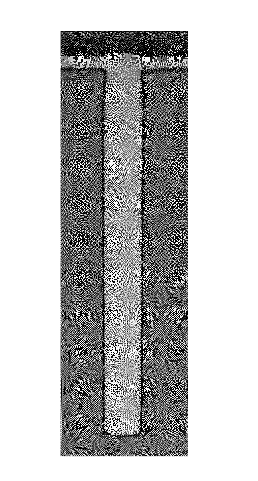
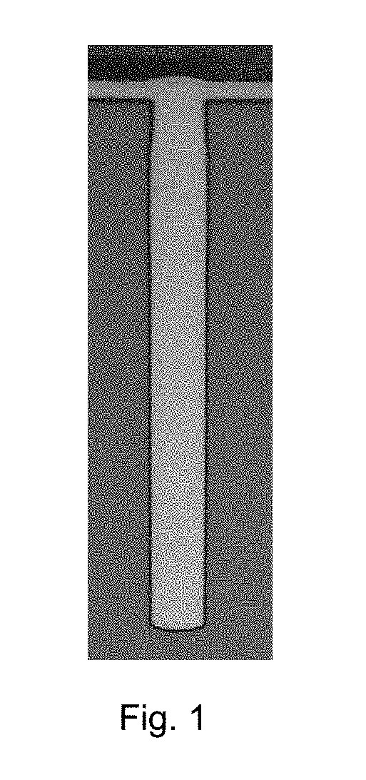
Image

Examples
preparation example 1
of the Inventive Additive
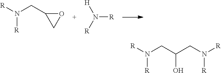
[0098]In a round bottom flask equipped with reflux condenser, a solution of 1.0 g 4,4′-Methylene-bis-(N,N-diglycidylaniline) (2.37 mmol, 1.0 eq.) in 120 ml water was prepared prior to the addition of 5.54 g Jeffamine M-600 (9.27 mmol, 3.9 eq.) thereto. The reaction mixture was stirred at 90° C. for 8 hours and then allowed to cool to room temperature. The solid product was isolated by filtration and washed with water. Yield was >90%. Finally, the solid was dissolved without further purification in 0.5 wt.-% sulphuric acid to obtain a 1 wt.-% solution.
preparation example 2
of Jeffamine M-600
[0099]A round bottom flask was charged with 15.0 g epichlorohydrin (162.1 mmol, 1.95 eq.) and the reactant was cooled in an ice bath. Then, 50.0 g Jeffamine M-600 (83.3 mmol, 1.0 eq.) was added slowly so that the temperature of the reaction mixture did not exceed 10° C. Upon complete addition of the second reactant, the reaction mixture was stirred at room temperature for 48 hours. Thereafter, the pH of the solution was adjusted to 7 with an aqueous sodium hydroxide solution (30% (m / v)). The reaction mixture was then extracted with 150 ml diethyl ether and the phase was washed 10 times with 50 ml water each. The ether-phase was subsequently dried over calcium chloride and the solvent was removed under reduced pressure. Finally, the clear viscous product was stored under nitrogen (>90%).
preparation example 3
[0100]In a round bottom flask equipped with reflux condenser, 3.0 g diglycidyl-Jeffamine M-600 (0.39 mmol, 1.0 eq.) were dissolved in 100 ml water. Then, 0.65 g iso-pentylamine (0.70 mmol, 1.8 eq.) was added to this solution. The reaction mixture was stirred at 90° C. for 8 hours. A suspension was formed which was cooled to room temperature before filtration. The solid product was washed with water. Yield was >90%. Finally, the solid was dissolved without further purification in 0.5 wt.-% sulphuric acid to obtain a 1 wt.-% solution.
[0101]Table 1 shows the reaction conditions for the preparation of the inventive additives following the procedure of preparation example 1. The molar ratio given in table 1 refers the molar ratio of aminoglycidyl compound to amine compound. In those cases where more than one amine compound was used the molar ratio is given based on the total amount of substance of all amine compounds listed.
[0102]The solvent given in table 1 is the media in which the rea...
PUM
| Property | Measurement | Unit |
|---|---|---|
| Time | aaaaa | aaaaa |
| Concentration | aaaaa | aaaaa |
| Concentration | aaaaa | aaaaa |
Abstract
Description
Claims
Application Information