Photodiode matrix with isolated cathodes

Inactive Publication Date: 2018-09-06
NEW IMAGING TECH
View PDF0 Cites 0 Cited by
  • Summary
  • Abstract
  • Description
  • Claims
  • Application Information

AI Technical Summary

Benefits of technology

[0017]It is one objective of the invention to propose a photodiode array and the method for manufacture thereof, allowing insulating of the cathodes from one another whilst maintaining good quantum yield and good surface yield of the array. With th

Problems solved by technology

However, it is difficult to work with a P-type substrate, and selective doping of N-type is ill controlled.
A shallower depth reduces the efficacy of photon absorption.
As a result, the pitch of the photodiodes on the surface of the array must be sufficiently large to allow an area 104 of Zn doping having portions of large width, and this approach

Method used


Image

  • Photodiode matrix with isolated cathodes
  • Photodiode matrix with isolated cathodes
  • Photodiode matrix with isolated cathodes

Examples


Embodiment Construction

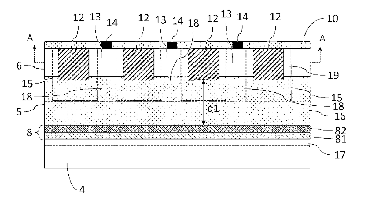
[0052]In the following description, as an illustrative example, the first type of conductivity is conductivity of N-type, whilst the second type of conductivity is conductivity of P-type. It would also be possible, by adapting the components, that the first type of conductivity is conductivity of P-type whilst the second type of conductivity is conductivity of N-type.

[0053]With reference to FIGS. 5 and 6, a photodiode array according to one embodiment of the invention comprises a substrate 4 of indium phosphide InP having conductivity of N-type, preferably N-doped i.e. with dopant elements of N-type such as silicon. For example, the concentration in terms of charge carriers of the substrate 4 may be between 1017 and 1019 cm−3.

[0054]The array also comprises an active layer 5 of indium gallium arsenide InGaAs constituting a photosensitive layer above the substrate 4. The thickness of the active layer is preferably greater than 3 μm and preferably less than 5 μm. The active layer 5 may...


PUM


Abstract

The invention relates to a photodiode matrix and to the method for manufacturing same, said matrix comprising a substrate (4) of indium phosphide an active layer (5) of indium gallium arsenide above the substrate (4), a buried region (8) between the substrate (4) and the active layer (5), and an upper layer (6) made of indium phosphide above the active layer (5), a photodiode anode made up of a doped region (12), said doped region (12) extending from the upper layer (6) into the active layer (5) without reaching the buried region (8), said doped region (12) defining a plurality of cathode areas (13) of the upper layer (6) isolated from one another by the doped region (12).

Description

FIELD OF THE INVENTION[0001]The invention relates to photodiode arrays and more particularly to photodiode arrays having layers of indium gallium arsenide (InGaAs) and indium phosphide (InP), and to the manufacturing method thereof.[0002]One of the methods for manufacturing a photodiode array in semiconductor materials with narrow band gap (often for detection in infrared light) is to insert the active detection layer with narrow band gap between two semiconductor materials with wide band gap. The two semiconductor layers with wide band gap consist of efficient protection / passivation whilst remaining transparent to the radiation wavelength intended to be detected by the photodiodes.[0003]In addition, with suitable doping, the two heterojunctions between the active layer and the two protection / passivation layers confine photoelectric charges within the active detection layer and improve the quantum yield of the photodiode thus formed.[0004]An InGaAs photodiode is a typical example of...

Claims


Application Information

Patent Timeline
IPC IPC(8): H01L27/146
CPCH01L27/14643H01L27/1463H01L27/14694H01L27/14649
Inventor NI, YANG
Owner NEW IMAGING TECH
Why Eureka
Try Eureka