Defect mitigation of thin-film hybrid perovskite and direct writing on a curved surface

a technology of thin-film hybrid perovskite and defect mitigation, which is applied in the manufacture of organic semiconductor devices, sustainable manufacturing/processing, and final product manufacturing. it can solve the problems of non-trivial transfer of device results derived from spin-coated photoactive layers in a standard laboratory setup to fabrication level devices

Active Publication Date: 2018-09-13
THE UNITED STATES OF AMERICA AS REPRESETNED BY THE SEC OF THE AIR FORCE
View PDF1 Cites 20 Cited by
  • Summary
  • Abstract
  • Description
  • Claims
  • Application Information

AI Technical Summary

Benefits of technology

[0007]According to one embodiment of the present invention, a controlled and efficient conversion of PbI2 to defect-free CH3NH3PbI3 thin-film by aerosol-jet printing (AJ) is described. The aerosol jet printer has attributes which are advantageous in the field of semiconductors and photovoltaics, including that it is a contactless printing approach, i.e. there is less damage of the underlying layers and applied layers, it is a scalable process, it deposits materials in the form of mist, which allows fine-tuning of material growth very precisely, and it enables the patterning of thin-film depositions. The ultrasonic transducer / atomizer is also an important part of the system. It helps to generate the mist of the precursor ink. In the alternative, it could be replaced by a pneumatic atomizer.

Problems solved by technology

Additionally, such photovoltaic devices are light weight, comprised of earth-abundant materials, and are chemically tunable.
To date, most demonstrations of this technology have been limited to lab scale and based on an extremely labor intensive manual spin-coating process in an inert atmosphere.
Unfortunately, the transfer of device results derived from spin-coated photoactive layers in a standard laboratory setup to fabrication level devices is non-trivial due to the enormous complexity of the thin-film perovskite growth dynamics and the lack of a generic protocol for fabricating high quality, high performing films which would ultimately lead to efficient solar cell devices.
Furthermore, the optimized perovskite solar cell performances for lab scale, spin-coated devices tend to be highly technique-sensitive as a result of the different mechanisms that drive the active layer film formation.

Method used


Image

  • Defect mitigation of thin-film hybrid perovskite and direct writing on a curved surface
  • Defect mitigation of thin-film hybrid perovskite and direct writing on a curved surface
  • Defect mitigation of thin-film hybrid perovskite and direct writing on a curved surface

Examples


Embodiment Construction

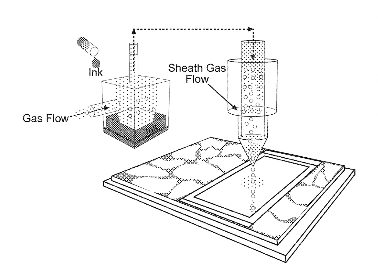
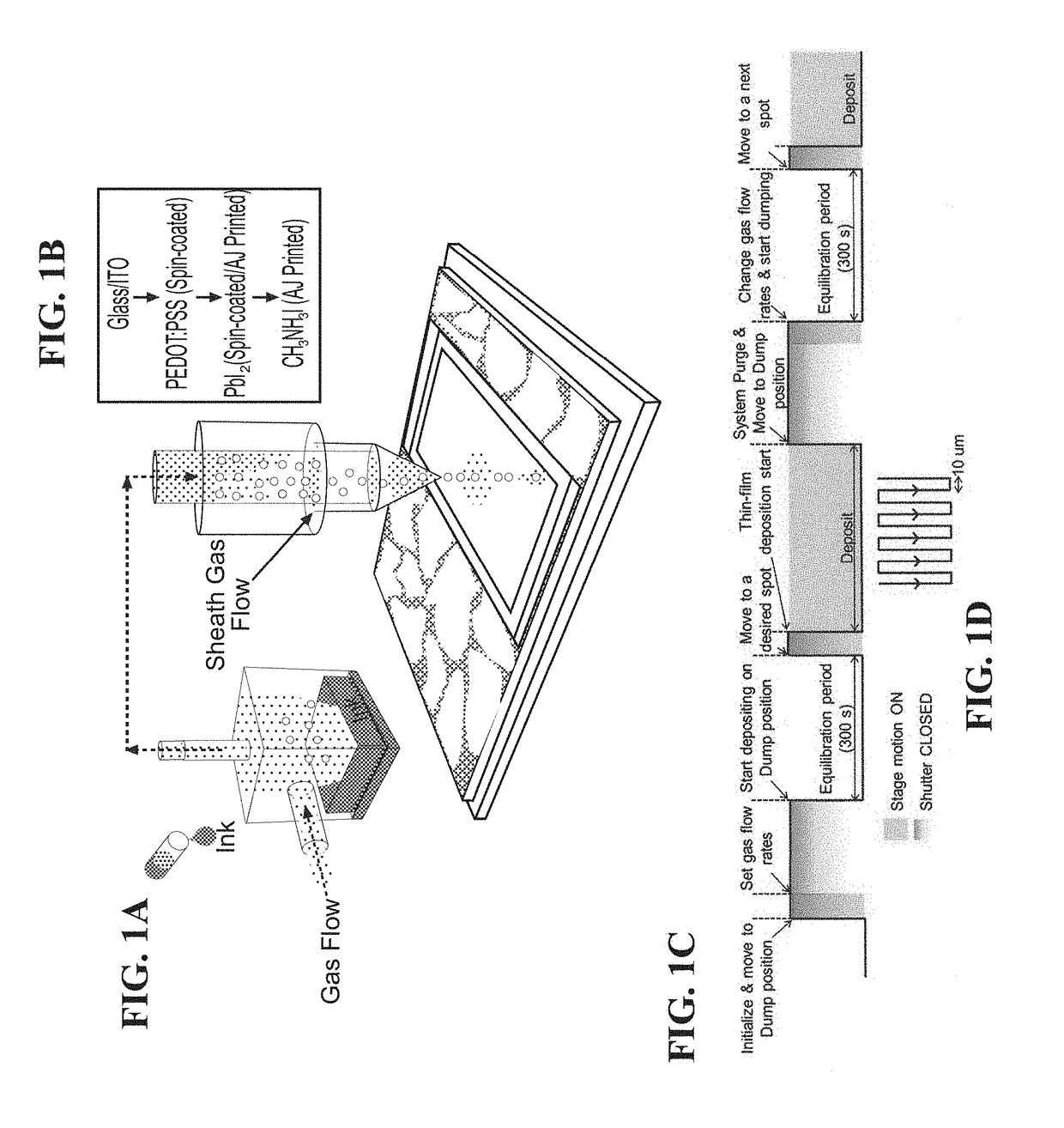
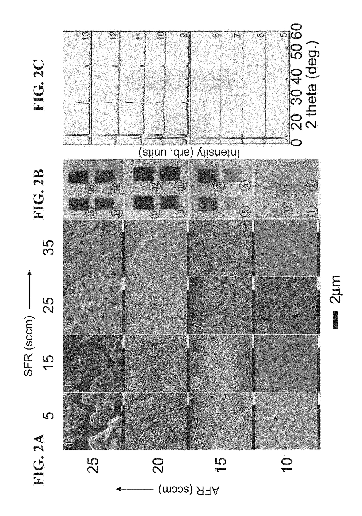
[0061]The performances of lab-scale, all spin-coated, methyl ammonium lead trihalide perovskite-based solar cell devices are subject to a near infinite level of variation based on individuals' expertise. The photovoltaic properties of perovskite solar cells are highly dependent on the active layer film morphology and crystallization, and as such the controlled deposition of defect-free perovskite films is of significant interest towards wide adoption of this inorganic-organic hybrid technology. Mitigating defects during an all-low temperature, solution processed perovskite thin-film growth through automation is highly desirable to facilitate the lab-to-fab process transfer of this emerging solar technology. Critical to this goal is the implementation of novel fabrication protocols which are robust and which have the advantage of full manufacturing compatibility. As a step forward, an aerosol-jet printing technique is presented herein for precisely controlling the thin-film perovskit...


PUM


Abstract

A method for aerosol jet printing a layered perovskite structure comprises applying a PEDOT:PSS layer to a substrate; applying a layer of lead iodide (PbI2) to the PEDOT:PSS layer; and applying an aerosol mist of methylammonium iodide (CH3NH3I) atop the PbI2 layer with an aerosol jet nozzle to form a CH3NH3PbI3 perovskite film layer. The substrate may be an ITO glass substrate, and the PEDOT:PSS layer may be applied by a process selected from spin-coating, inkjet-printing, slot-die-coating, aerosol jet printing, physical vapor deposition, chemical vapor deposition, and electrochemical deposition. The PbI2 layer may be applied by a process selected from spin-coating, aerosol jet printing, inkjet-printing, slot-die-coating, physical vapor deposition, chemical vapor deposition, and electrochemical deposition, and the PbI2 for application to the PEDOT:PSS layer may be in a solution of DMF, DMSO, γ-butyrolactone, or a combination thereof. The annealing of the PbI2 layer may be performed at about 80° C. or lower.

Description

[0001]Pursuant to 37 C.F.R. § 1.78(a)(4), this application claims the benefit of and priority to prior filed co-pending Provisional Application Ser. No. 62 / 468,734, filed 8 Mar. 2017, which is expressly incorporated herein by reference.RIGHTS OF THE GOVERNMENT[0002]The invention described herein may be manufactured and used by or for the Government of the United States for all governmental purposes without the payment of any royalty.FIELD OF THE INVENTION[0003]The present invention relates generally to the manufacture of thin-film hybrid perovskite semiconductors and, more particularly, to the mitigation of defects of thin-film hybrid perovskite semiconductor-based photovoltaics, even when they are written directly on a curved surface.BACKGROUND OF THE INVENTION[0004]Disruptive photovoltaic (PV) technologies that imitate the principles of digital printing as a means of manufacturing devices offer the promise of low-cost along with the advantages of unique form factors and high throu...

Claims


Application Information

Patent Timeline
Patent Type & Authority Applications(United States)
IPC IPC(8): H01G9/20H01L51/00H01L51/42
CPCH01G9/20H01L51/0096H01L51/0013H01L51/0028H01L51/4293H01L51/424H01L2251/308Y02E10/549Y02P70/50H10K71/15H10K71/18H10K85/1135H10K30/50H10K30/20H10K30/40H10K71/441H10K77/10H10K2102/103
Inventor BAG, SANTANUDENEAULT, JAMES R.DURSTOCK, MICHAEL F.
Owner THE UNITED STATES OF AMERICA AS REPRESETNED BY THE SEC OF THE AIR FORCE
Why Eureka
Try Eureka