Hybrid growth method for iii-nitride tunnel junction devices

a tunnel junction and hybrid technology, applied in the direction of crystal growth process, crystal growth process, polycrystalline material growth, etc., can solve the problems of low hole concentration and mobility, inability to use p-gan as a current spreading layer, difficult contact with nitride (p-gan) electrically, etc., to achieve better tunnel junctions, reduce the operating voltage of these devices, and increase efficiency

Active Publication Date: 2019-03-07
RGT UNIV OF CALIFORNIA
View PDF5 Cites 11 Cited by
  • Summary
  • Abstract
  • Description
  • Claims
  • Application Information

AI Technical Summary

Benefits of technology

[0013]To overcome the limitations in the prior art described above, and to overcome other limitations that will become apparent upon reading and understanding this specification, the present invention discloses a hybrid growth method for III-nitride tunnel junction devices, wherein MOCVD, which may be plasma MOCVD, is used to grow one or more light-emitting or light-absorbing structures, and ammonia-assisted or plasma-assisted molecular beam epitaxy (MBE) is used to grow one or more tunnel junctions. Unlike p-GaN grown by MOCVD, p-GaN grown by MBE is conductive as grown, which would allow for its use in a tunnel junction. Additionally, the doping limits of MBE materials are higher than MOCVD materials, which allows for better tunnel junctions. By combining MOCVD grown light emitters or absorbers and MBE grown

Problems solved by technology

However, p-type gallium nitride (p-GaN) is difficult to contact electrically, and has low hole concentration and mobility.
This means that p-GaN cannot be used as a current spreading layer and that traditional p-contacts will add significant voltage to devices.
However, there have been a number of difficulties in achieving high quality tunnel junctions in the GaN mater

Method used


Image

  • Hybrid growth method for iii-nitride tunnel junction devices
  • Hybrid growth method for iii-nitride tunnel junction devices
  • Hybrid growth method for iii-nitride tunnel junction devices

Examples


Embodiment Construction

[0034]In the following description of the preferred embodiment, reference is made to a specific embodiment in which the invention may be practiced. It is to be understood that other embodiments may be utilized and structural changes may be made without departing from the scope of the present invention.

[0035]Overview

[0036]As noted above, the present invention comprises a hybrid growth method for III-nitride tunnel junction devices that uses MOCVD to grow one or more light-emitting or light-absorbing structures and MBE is used to grow one or more tunnel junctions.

[0037]Epitaxial Structures

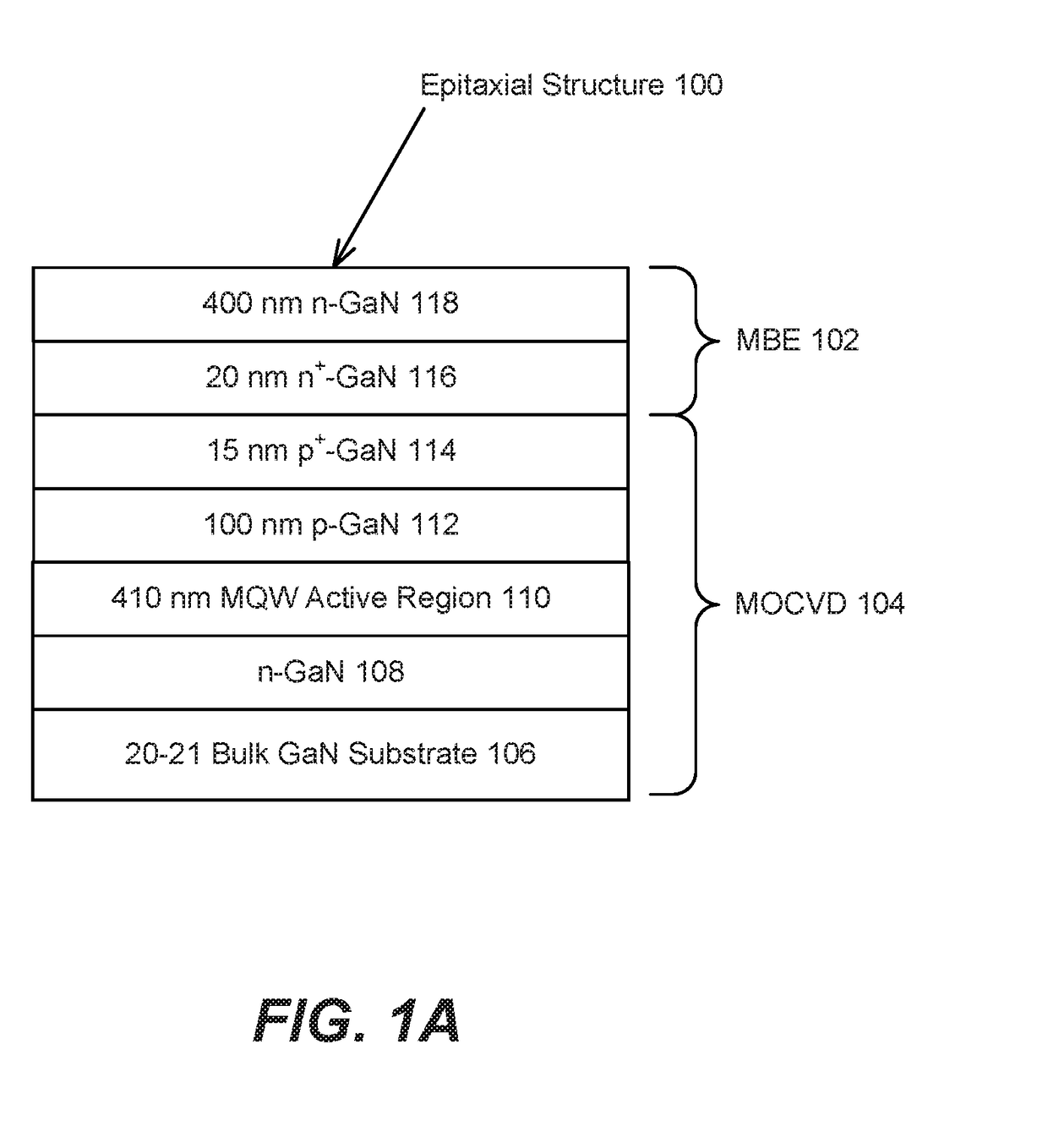
[0038]To demonstrate the tunnel junction design according to the present invention, 410 nm emitting LEDs were grown by MOCVD on 20-21 bulk GaN substrates with a 15 nm p+-GaN cap as the final layer. The epitaxial structure 100 is shown in FIG. 1A, which illustrates an MBE tunnel junction grown on an MOCVD LED, wherein the layers of the structure 100 are annotated by their respective MBE 102 or MOCVD 1...


PUM


Abstract

A hybrid growth method for III-nitride tunnel junction devices uses metal-organic chemical vapor deposition (MOCVD) to grow one or more light-emitting or light-absorbing structures and ammonia-assisted or plasma-assisted molecular beam epitaxy (MBE) to grow one or more tunnel junctions. Unlike p-type gallium nitride (p-GaN) grown by MOCVD, p-GaN grown by MBE is conductive as grown, which allows for its use in a tunnel junction. Moreover, the doping limits of MBE materials are higher than MOCVD materials. The tunnel junctions can be used to incorporate multiple active regions into a single device. In addition, n-type GaN (n-GaN) can be used as a current spreading layer on both sides of the device, eliminating the need for a transparent conductive oxide (TCO) layer or a silver (Au) mirror.

Description

CROSS REFERENCE TO RELATED APPLICATION[0001]This application claims the benefit under 35 U.S.C Section 119(e) of the following co-pending and commonly-assigned application:[0002]U.S. Provisional Application Ser. No. 62 / 190,929, filed on Jul. 10, 2015, by Erin C. Young, Benjamin P. Yonkee, John T. Leonard, Tal Margalith, James S. Speck, Steven P. DenBaars, and Shuji Nakamura, entitled “HYBRID GROWTH METHOD FOR III-NITRIDE TUNNEL JUNCTION DEVICES,” attorneys' docket number 30794.588-US-P1 (2015-904-1);[0003]which application is incorporated by reference herein.BACKGROUND OF THE INVENTION1. Field of the Invention[0004]This invention relates to a hybrid growth method for III-nitride tunnel junction devices.2. Description of the Related Art[0005](Note: This application references a number of different publications as indicated throughout the specification by one or more reference numbers in brackets, e.g., [x]. A list of these different publications ordered according to these reference n...

Claims


Application Information

Patent Timeline
IPC IPC(8): H01L33/00H01L33/06H01L33/32H01L31/147
CPCH01L33/0075H01L33/06H01L33/32H01L31/147H01L21/00H01L33/14H01L31/03044C30B25/20C30B29/406H01L21/02458H01L21/0254H01L21/0262H01L21/02631H01L33/04C30B23/025C30B29/68H01L21/02505H01S5/0262H01S5/183H01S5/3095H01S5/34333H01S5/4043Y02E10/544
Inventor YOUNG, ERIN C.YONKEE, BENJAMIN P.LEONARD, JOHN T.MARGALITH, TALSPECK, JAMES S.DENBAARS, STEVEN P.NAKAMURA, SHUJI
Owner RGT UNIV OF CALIFORNIA
Why Eureka
Try Eureka