A High-electron-mobility transistor (HEMT)

a high-electron mobility, transistor technology, applied in the direction of semiconductor devices, semiconductor/solid-state device details, electrical apparatus, etc., can solve the problems of not being able to contact the outside world, unable to achieve the effect of reducing the cost unable to achieve the effect of a single transistor,

Active Publication Date: 2019-03-14
INDIAN INSTITUTE OF SCIENCE
View PDF1 Cites 19 Cited by
  • Summary
  • Abstract
  • Description
  • Claims
  • Application Information

AI Technical Summary

Benefits of technology

[0016]Another object of the present disclosure is to present a GaN HEMT that improves the short channel effects and hence gate control over channel.
[0017]Another object of the present disclosure is to present a GaN HEMT that increases switching speed for a given breakdown voltage.
[0018]Another object of the present disclosure is to present a GaN HEMT that improves device reliability.
[0019]Another object of the present disclosure is to present a GaN HEMT that reduces device foot print, hence lowers the cost.
[0020]Another object of the present disclosure is to present a GaN HEMT that reduces gate field plate length; hence lowers gate-to-drain (miller) capacitance.

Problems solved by technology

Moreover, since the gate is 50-100 nm away from the 2DEG, the gate to channel control suffers in this architecture.
Hence, this architecture is expected to suffer from slower turn-on and larger gate voltage swing for switching operation, which can also add to dynamic or turn-on losses.
Gate and source of HEMT and drain of Si-LDMOS are tied together, however are not available for contacting to outside world.
Due to cascode operation, device performance is expected to be lower and limited to channel characteristics of Si-LDMOS device when compared to e-mode GaN HEMT.
Last but not the least, this configuration is known to be less reliable both under extended stress as well as under short circuit stress conditions.
However, such device includes certain technical drawbacks and hence may not technically fit to provide desired functionalities.
One of the major technical problems available in the device of U.S. Pat. No. 7,449,762 B1 is attributed to gate stack being directly in contact with P—GaN layer, making channel formation in this device very slow.
Moreover, due to unavailability of minority carriers (electrons) in P—GaN buffer, formed channel electron density will be very small (can be almost negligible depending of P—GaN doping), which will give rise to ON resistance.
Also, high breakdown voltage would require higher P—GaN doping, however this can deplete 2DEG.

Method used


Image

  • A High-electron-mobility transistor (HEMT)
  • A High-electron-mobility transistor (HEMT)
  • A High-electron-mobility transistor (HEMT)

Examples


Embodiment Construction

[0065]The following is a detailed description of embodiments of the disclosure depicted in the accompanying drawings. The embodiments are in such detail as to clearly communicate the disclosure. However, the amount of detail offered is not intended to limit the anticipated variations of embodiments; on the contrary, the intention is to cover all modifications, equivalents, and alternatives falling within the spirit and scope of the present disclosure as defined by the appended claims.

[0066]Various terms as used herein are shown below. To the extent a term used in a claim is not defined below, it should be given the broadest definition persons in the pertinent art have given that term as reflected in printed publications and issued patents at the time of filing.

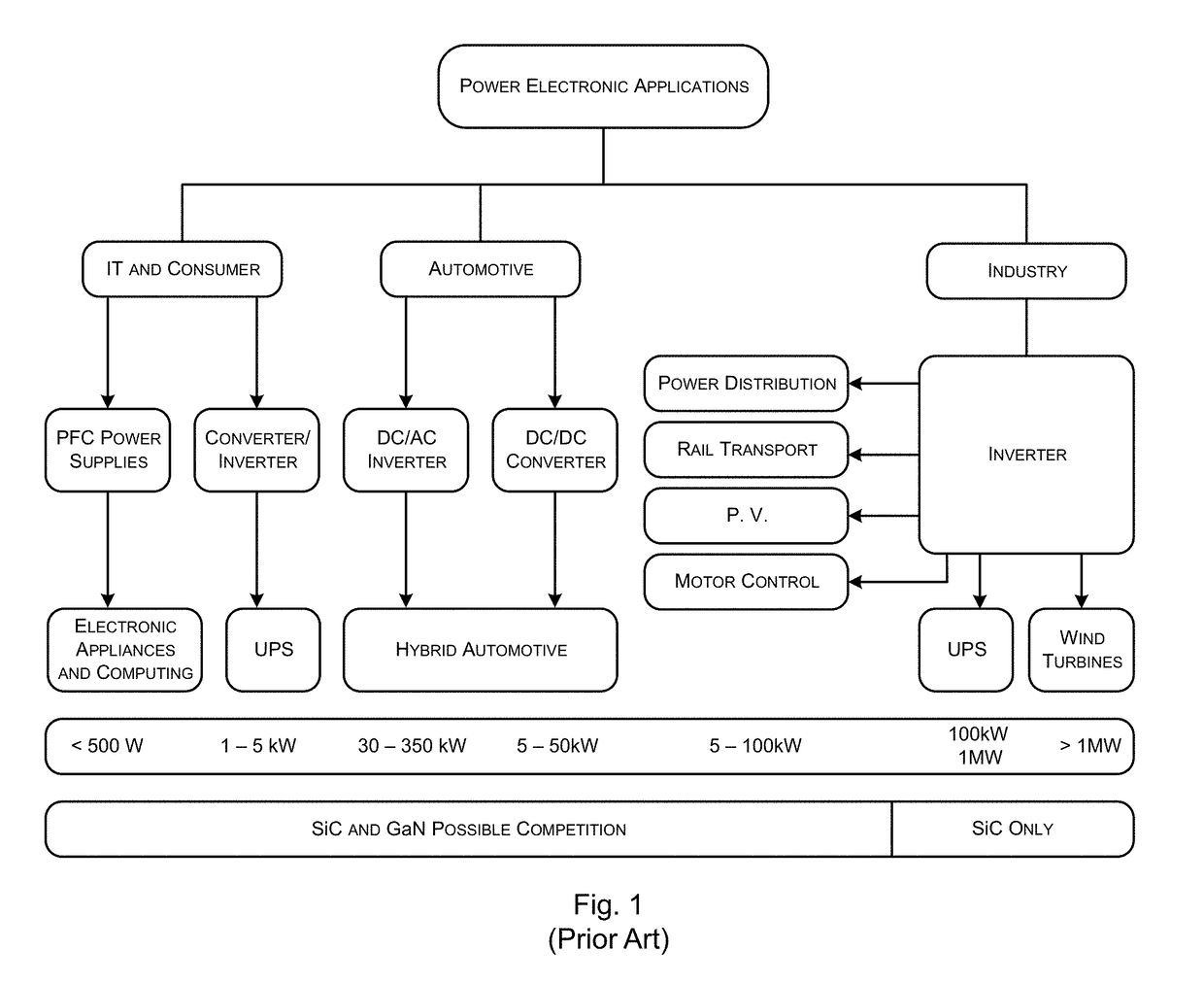
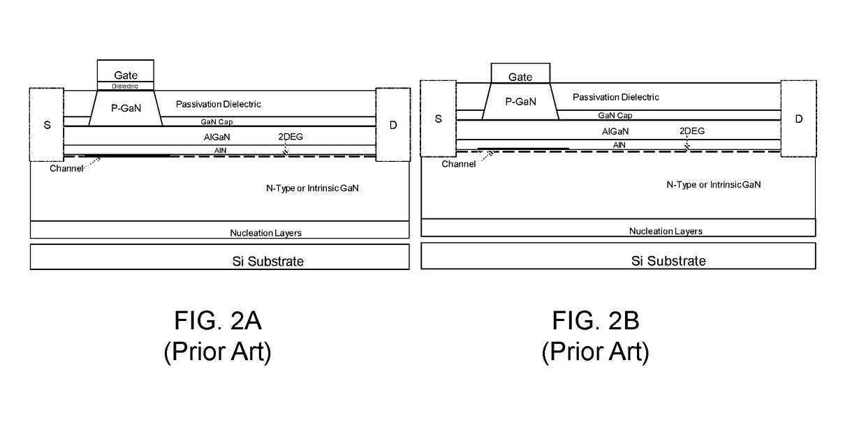
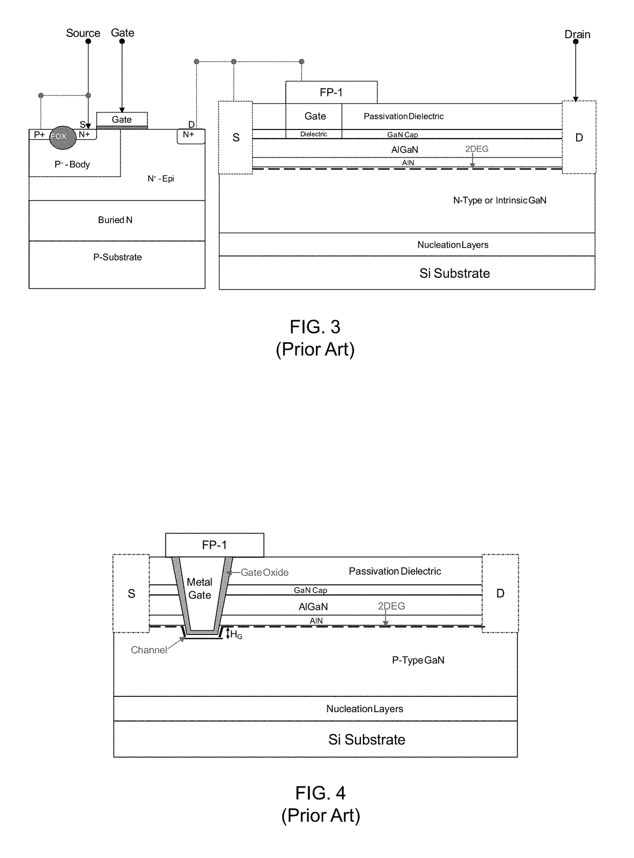
[0067]The present disclosure relates generally to devices having elements operating with a 2-dimension electron gas (2DEG), and relates in particular to recess gate superjunction (SJ) high-electron-mobility transistor (HEMT) o...


PUM


Abstract

The present disclosure provides a superjunction based design for normally-OFF HEMT that has two key components: (i) a recessed high-K metal gate and (ii) a superjunction layer under the gate, which is embedded within the N-type GaN buffer layers and separated from recessed gate. Recess gate is to deplete the 2DEG from the channel region (under the gate) when the transistor is under OFF state. The present disclosure provides a new, improved, efficient and technically advanced HEMT device which can provide higher breakdown voltage, when compared to designs available in the prior-art, without affecting the performance figure of merits. Further, the new HEMT device offers improved breakdown voltage as compared to ON-resistance trade-off, improved the short channel effects, improved gate control over channel, improved switching speed for a given breakdown voltage, and improved device reliability. Furthermore, the new HEMT device lowers gate-to-drain (miller) capacitance and is available at low cost.

Description

TECHNICAL FIELD[0001]The present disclosure relates generally to transistors. In particular the present disclosure relates to a high electron mobility transistor having an engineered buffer layer for reduced surface field (RESURF).BACKGROUND[0002]Background description includes information that may be useful in understanding the present invention. It is not an admission that any of the information provided herein is prior art or relevant to the presently claimed invention, or that any publication specifically or implicitly referenced is prior art.[0003]Power electronics is an application of solid-state electronics for control and conversion of electric power. Power electronic products capture a big majority of electronics market share today, which is attributed to diverse range of applications they cater to, which in turn is enabled by advance power semiconductor device technologies. As well known in the art, semiconductor devices are electronic components that exploit electronic pr...

Claims


Application Information

Patent Timeline
Patent Type & Authority Applications(United States)
IPC IPC(8): H01L29/778H01L29/20H01L23/31H01L29/06H01L21/768
CPCH01L29/778H01L29/2003H01L23/3171H01L29/0634H01L21/76832H01L29/402H01L29/404H01L29/41766H01L29/4236H01L29/7786
Inventor SHRIVASTAVA, MAYANK
Owner INDIAN INSTITUTE OF SCIENCE
Why Eureka
Try Eureka