GaN TRANSISTOR WITH INTEGRATED DRAIN VOLTAGE SENSE FOR FAST OVERCURRENT AND SHORT CIRCUIT PROTECTION

Active Publication Date: 2019-05-09
GAN SYST
View PDF2 Cites 14 Cited by
  • Summary
  • Abstract
  • Description
  • Claims
  • Application Information

AI Technical Summary

Benefits of technology

[0009]The present invention seeks to provide integrated overcurrent and short circuit protection for devices and systems comprisin

Problems solved by technology

Industry standard OCP options for IGBTs (Insulated Gate Bipolar Transistors) are typically too slow for protecting faster GaN power devices.
For example, the following methods for overcurrent protection are known: De-saturation detection: widely used for SiC IGBTs; however, this method of OCP is slow and may not meet the requirements for Ga

Method used


Image

  • GaN TRANSISTOR WITH INTEGRATED DRAIN VOLTAGE SENSE FOR FAST OVERCURRENT AND SHORT CIRCUIT PROTECTION
  • GaN TRANSISTOR WITH INTEGRATED DRAIN VOLTAGE SENSE FOR FAST OVERCURRENT AND SHORT CIRCUIT PROTECTION
  • GaN TRANSISTOR WITH INTEGRATED DRAIN VOLTAGE SENSE FOR FAST OVERCURRENT AND SHORT CIRCUIT PROTECTION

Examples


Example

EXAMPLE

OCP for Large Area, High Voltage / High Current GaN E-HEMT with Integrated Drain Voltage Sense

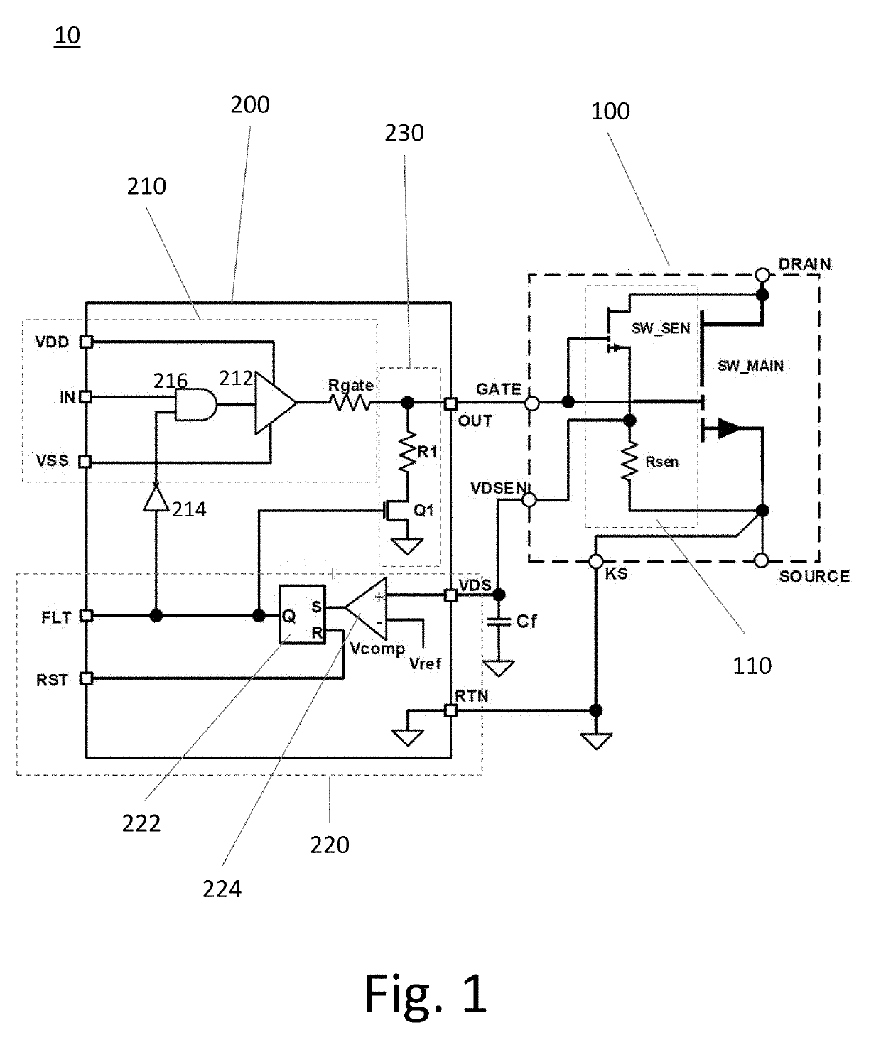
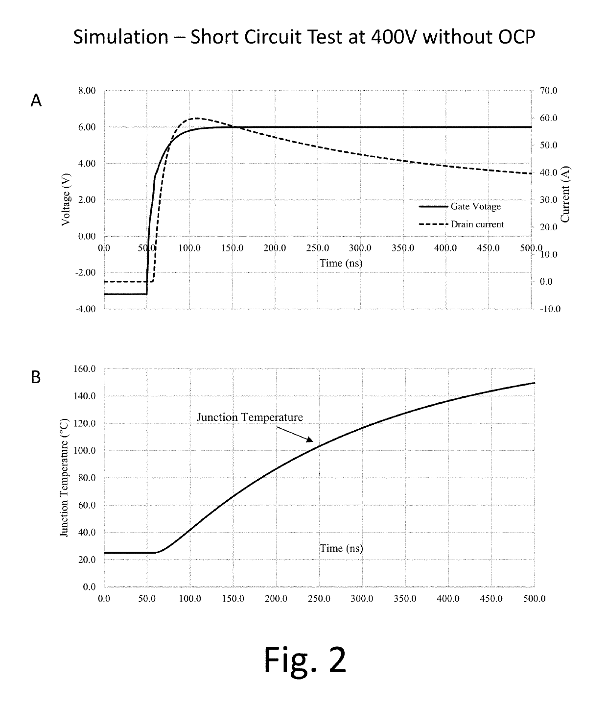
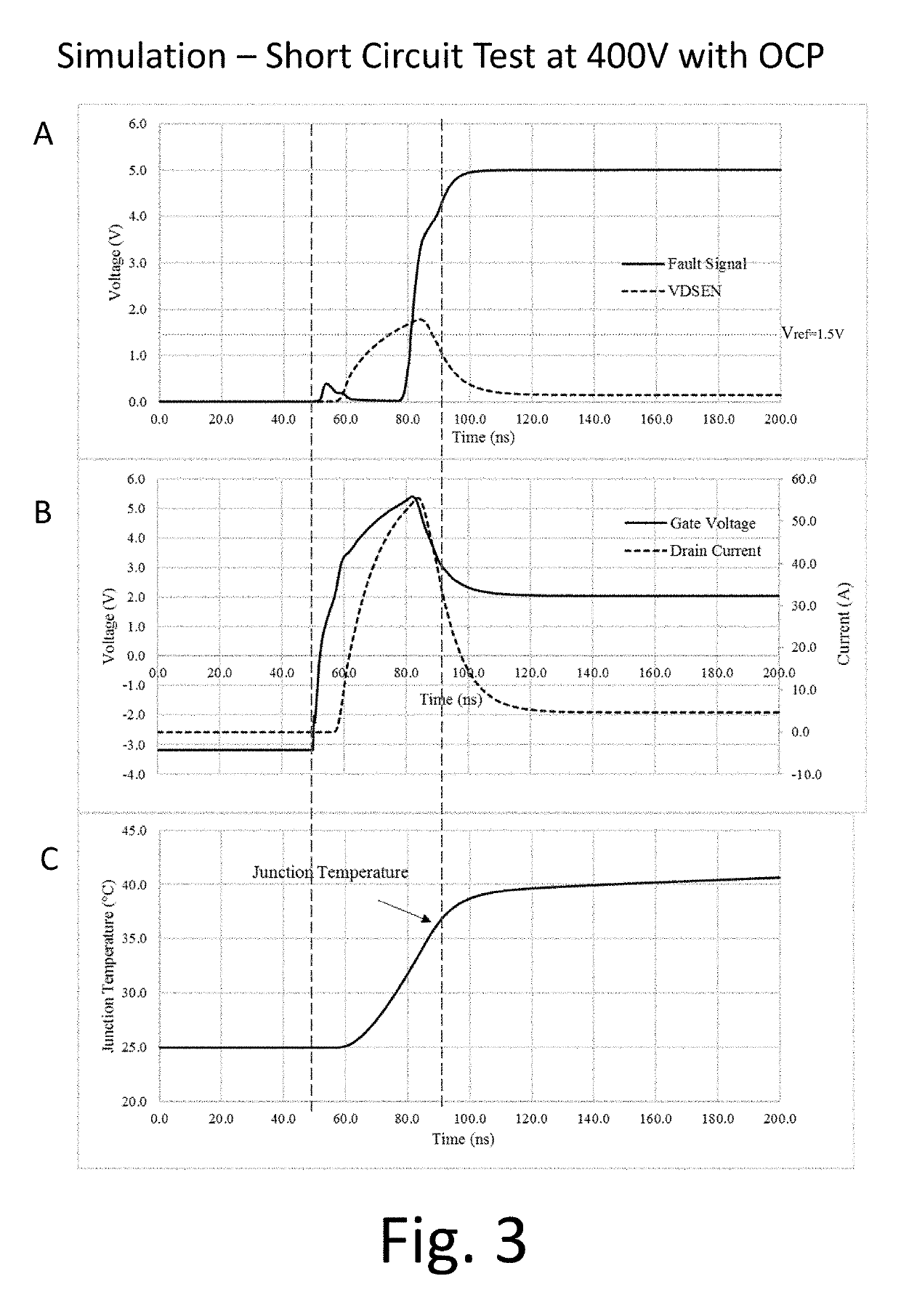
[0040]The operation of the system illustrated in FIG. 1 will be described in more detail, by way of example, with reference to simulation results based on a lateral GaN power switch SW_MAIN, which comprises a large area, large gate width lateral GaN E-HEMT. Simulation results for a GaN E-HEMT in the form of a 650V / 50 mΩ device which has a gate width Wg=300 mm and a drain-source on-resistance, Rdson, of 50 mΩ are shown in FIGS. 2 to 4.

[0041]It is desirable that the drain voltage sensing circuit 110 takes up minimal space on the GaN die 100 and that SW_SEN and Rsen are small enough so that they carry a small proportion of the current carried by the GaN switch SW_MAIN, for example a current of only tens of mA. On the other hand, since Rsen is part of the SW_SEN gate resistor that controls or limits the switching speed of SW_SEN, the gate widths of SW_SEN and Rsen should be large enough pr...


PUM


Abstract

A GaN transistor switch SW_MAIN has an integrated drain voltage sense circuit, which provides a drain voltage sense signal VDSEN. The integrated drain voltage sense circuit comprises GaN sense transistor SW_SEN and GaN sense resistor RSEN, which form a resistive divider for sensing the drain voltage of SW_MAIN, and generating the drain sense voltage output VDSEN. Fault detection logic circuitry of a driver circuit generates a fault signal FLT when VDSEN reaches or exceeds a reference voltage Vref, which triggers fast turn-off of the gate of SW_MAIN within less than 100 ns of an overcurrent or short circuit condition. During turn-off, RSEN resets to VDSEN=0. For two stage turn-off, the driver circuit further comprises fast soft turn-off circuitry which is triggered first by the fault signal to pull-down the gate voltage to the threshold voltage, followed by a delay before full turn-off of the gate SW_MAIN by the gate driver.

Description

CROSS-REFERENCE TO RELATED APPLICATION(S)[0001]N / ATECHNICAL FIELD[0002]The present invention relates to overcurrent and short circuit protection for devices and systems comprising gallium nitride (GaN) transistors, including GaN power switches, such as, high current / high voltage GaN High Electron Mobility Transistors (GaN HEMTs).BACKGROUND ART[0003]Fast wide bandgap semiconductor power devices, such as Silicon Carbide (SiC) or Gallium Nitride (GaN) transistors require fast short circuit and overcurrent protection (OCP). Industry standard OCP options for IGBTs (Insulated Gate Bipolar Transistors) are typically too slow for protecting faster GaN power devices. The thermal mass of a lateral GaN HEMT is small; e.g., during a short circuit or overcurrent, a lateral GaN HEMT may heat up very quickly and have a survival time of only 300 ns to 500 ns. An IGBT is typically more robust and can survive a few microseconds.[0004]For example, the following methods for overcurrent protection are k...

Claims


Application Information

Patent Timeline
IPC IPC(8): H03K17/081H01L29/20H01L29/423H01L29/778
CPCH03K17/08104H01L29/2003H01L29/42316H01L29/7787H01L27/0605H01L27/0629H01L28/20H01L25/18H03K17/0822H03K17/163
Inventor CHEN, DISPAZIANI, LARRY
Owner GAN SYST
Why Eureka
Try Eureka