Process for the preparation of halide perovskite and perovskite-related materials

a technology of halide perovskite and related materials, which is applied in the direction of lead halides, solid-state diffusion coatings, liquid/solution decomposition chemical coatings, etc., can solve the problems of increasing manufacturing costs, less popular methods, and toxic sprayed liquids

Inactive Publication Date: 2019-06-20
YEDA RES & DEV CO LTD
View PDF0 Cites 15 Cited by
  • Summary
  • Abstract
  • Description
  • Claims
  • Application Information

AI Technical Summary

Benefits of technology

[0050]In one embodiment, this invention is directed to a method for the preparation of halide perovskite or perovskite-related material. The main advantage of this invention is the reduced toxicity of the solution used in the process. Additionally, the metals (mainly Pb) are much less toxic in terms of manufacturing than the salts of the same metals. Further advantages are the preparation simplicity and a good morphology control of the perovskites prepared by the methods of this invention. This invention provides direct conversion of an elemental metal or alloy to a halide perovskite or perovskite related material.

Problems solved by technology

Therefore toxicity would be an important consideration at the manufacturing stage, which could increase considerably the manufacturing costs.
This method is, though, less popular mainly due to its higher level of complexity and high-energy input.
Very often the sprayed liquid is very toxic, which is the case with spray coating of perovskites.
Usually such systems require high level of isolation from the environment.

Method used


Image

  • Process for the preparation of halide perovskite and perovskite-related materials
  • Process for the preparation of halide perovskite and perovskite-related materials
  • Process for the preparation of halide perovskite and perovskite-related materials

Examples


example 1

Conversion of Metallic Lead (Pb) to MAPbX3

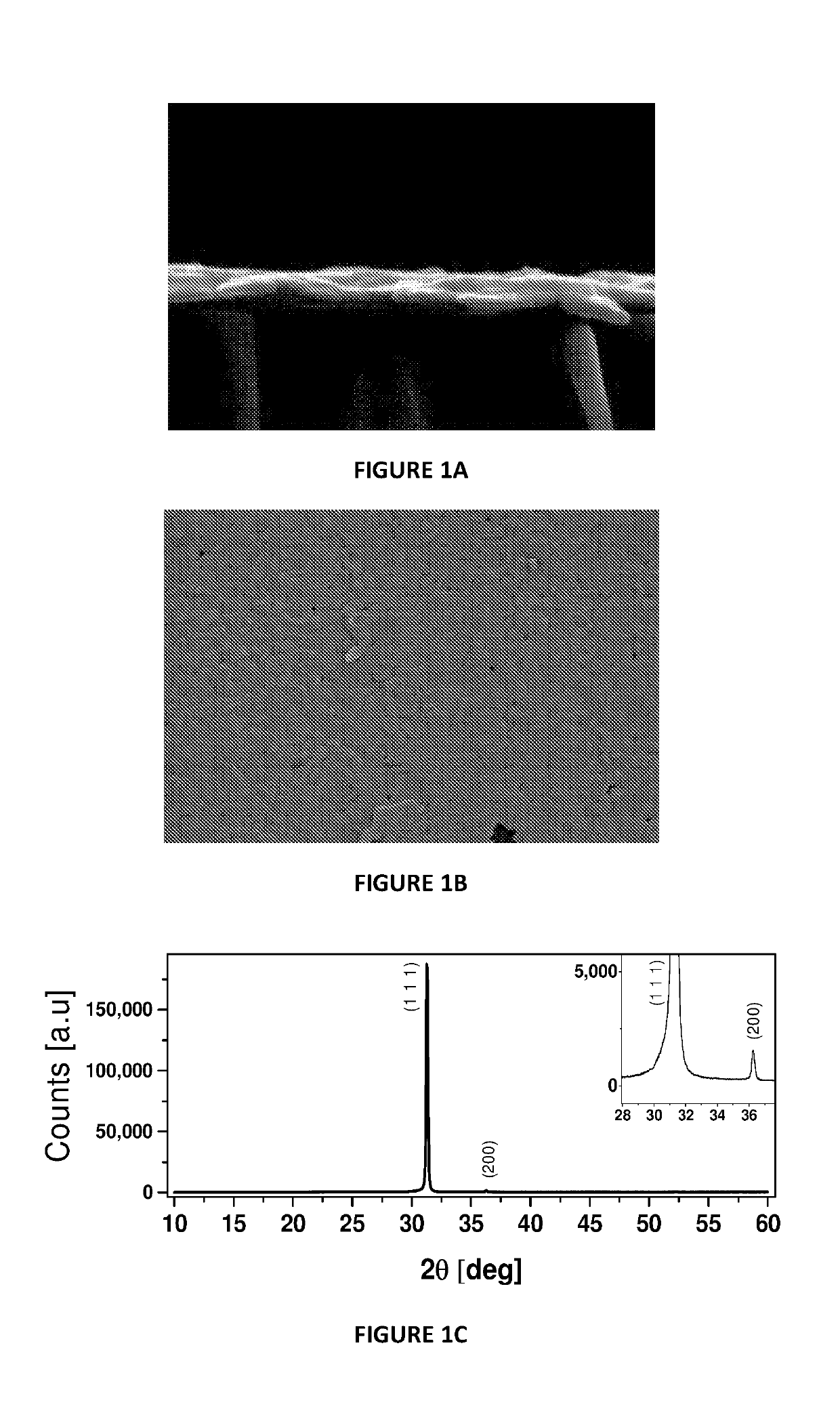
[0133]Thermal evaporation of Pb was carried out on three different substrates.[0134]Glass microscope slide[0135]Dense-TiO2 on top of fluorine-doped tin oxide (FTO)-coated glass (d-TiO2).[0136](100) p-type (boron doped) Si

[0137]In all three cases a shiny layer of Pb metal with controlled thickness was obtained. Powder X-ray diffraction (XRD) and scanning electron microscope (SEM) images (

[0138]FIGS. 1A-D) and concentration optimization to roughly optimize morphology were done with ˜50 or ˜120 nm thick evaporated Pb.

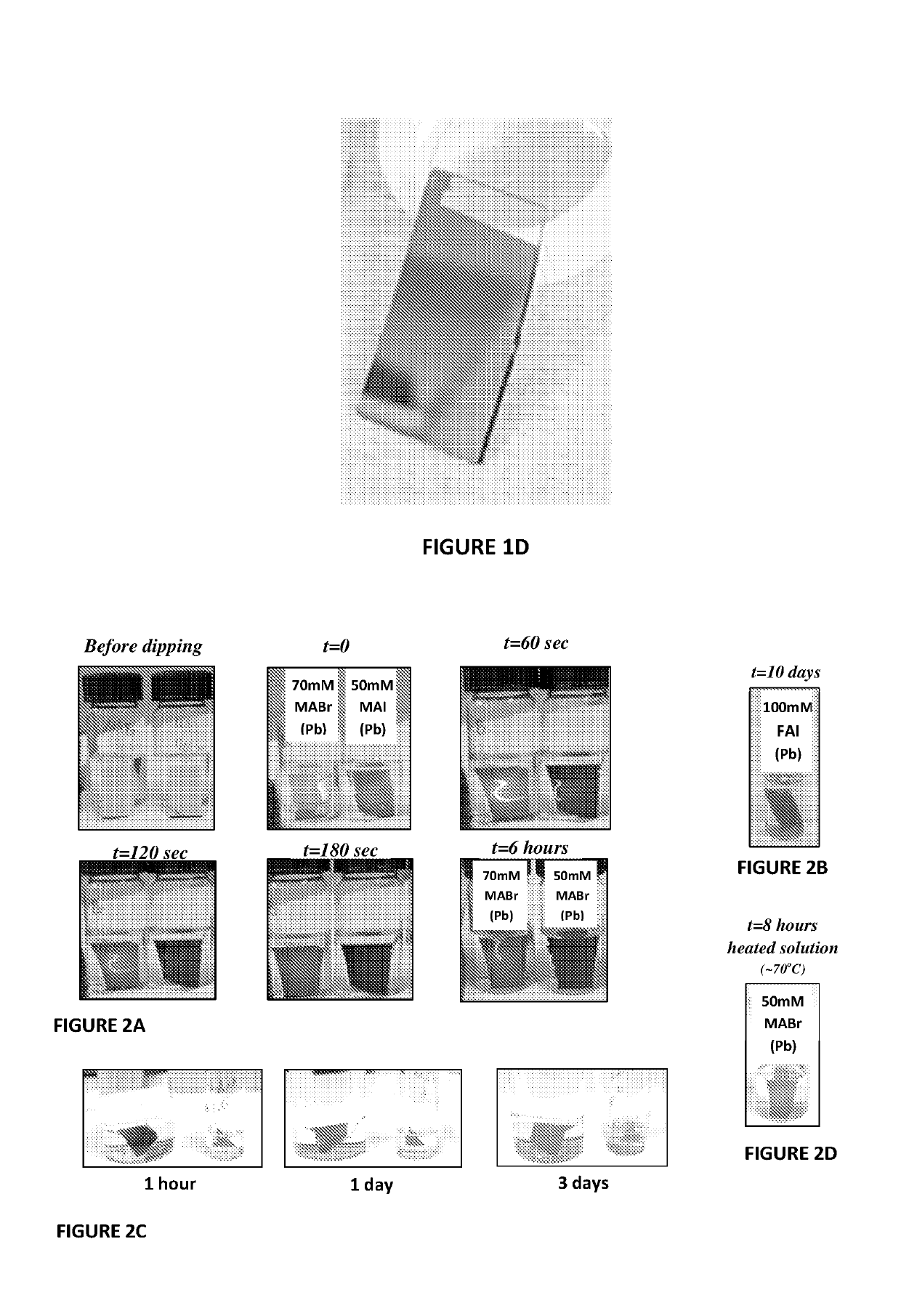
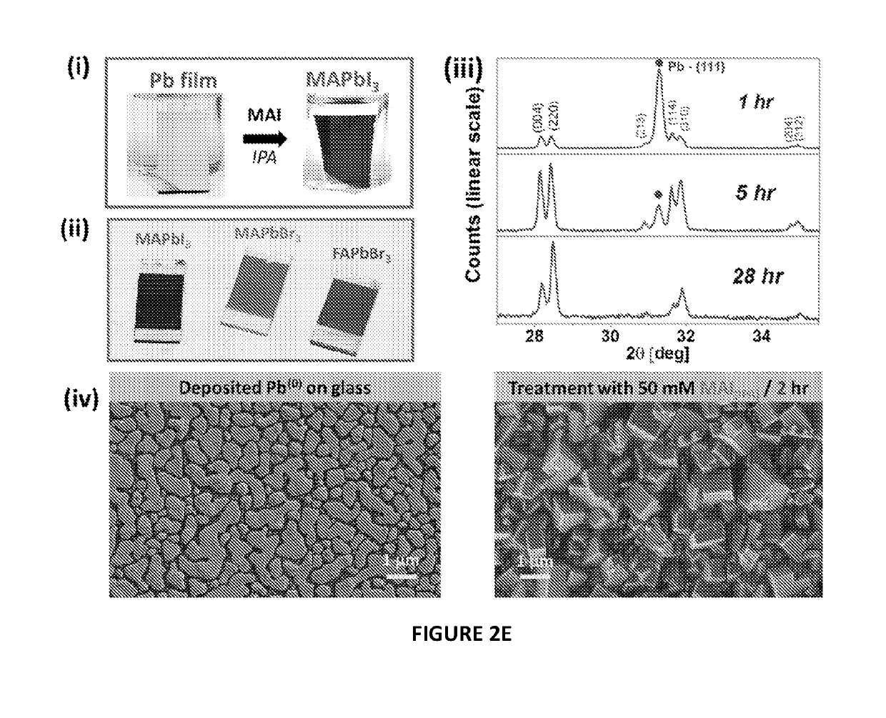
[0139]The evaporated Pb layers were placed in vials filled with various alcoholic solutions of 0.05-0.1M methylammonium iodide (MAI), methylammonium bromide (MABr) and formamidinium iodide (FAI). Methanolic solutions of MAI reacted extremely rapidly and essentially etched the layers from the substrate. Ethanolic MAI converted the shiny silver-gray Pb layer to a black coating. The reaction at room temperature began immediately. How...

example 2

The Effect of MAX (X=Br, I) Concentration on the Film Layer Morphology of MAPbX3

[0151]The effect of MAX (X=Br, I) concentration on the film morphology is shown in

[0152]FIGS. 4A-4E for 5 different concentrations: 500 mM, 200 mM, 100 mM 50 mM and 20 mM of MAX. Two effects of increasing the salt concentration that are seen immediately, were a decrease in crystal size and increasing non-uniformity of the film. Another effect was that cracking of the films occurred at the higher concentrations. For solar cell purposes, an optimum between large crystals and good coverage (smaller crystals) occurs at concentrations of 50-70 mM.

[0153]The film morphology is very important in determining the film properties. The desired morphology depends on the intended use of the films or material.

example 3

The Effect of Temperature and Solvent on Film Layer Morphology of MAPbX3

[0154]Lower temperature treatment gave better overall coverage (FIG. 7C) while higher temperature gave on average larger and more anisotropic crystals (FIG. 5). Treatment in ethanol instead of IPA gave much larger crystals but poorer coverage (FIG. 10A, 10B).


PUM

PropertyMeasurementUnit
optical band gapsaaaaaaaaaa

Abstract

This invention is related to a method for the preparation of halide perovskite or perovskite-related materials on a substrate and to optoelectronic devices and photovoltaic cells comprising the perovskites prepared by the methods of this invention The method for the preparation of the perovskite includes a direct conversion of elemental metal or metal alloy to halide perovskite or perovskite-related materials.

Description

FIELD OF THE INVENTION[0001]This invention is related to a method for the preparation of halide perovskite or perovskite-related materials on a substrate and to optoelectronic devices and photovoltaic cells comprising the perovskites prepared by the methods of this invention. The method for the preparation of the perovskite includes a direct conversion of elemental metal or metal alloy to halide perovskite or perovskite-related materials.BACKGROUND OF THE INVENTION[0002]Halide perovskite semiconductors have demonstrated unusual rapid progress in photovoltaic performance, now surpassing 20% conversion efficiency. While these materials have been known for a long time, it is only in the past ˜25 years that they have been seriously considered as electronic materials, in particular as light-emitting devices and transistors [1] while their entry into photovoltaic research occurred only a few years ago (2012) [2-5].[0003]The most studied material is MAPbI3 since this material has a bandgap...

Claims


Application Information

Patent Timeline
Patent Type & Authority Applications(United States)
IPC IPC(8): C07F7/24C07F7/22C01G21/16H01L51/00
CPCC07F7/24C07F7/2288C07F7/2284C01G21/16H01L51/005H01L51/4226H01L2251/301C01P2002/34C25D3/30C25D3/34C23C8/40C30B7/14C30B25/00C30B29/12C23C18/31Y02E10/549C25D5/48C23C18/1689H10K85/00H10K85/60H10K30/151H10K85/50H10K2102/00
Inventor CAHEN, DAVIDMODES, GARYRAKITA, YEVGENYKEDEM, NIR
Owner YEDA RES & DEV CO LTD
Why Eureka
Try Eureka