Semiconductor device and power conversion device

a technology of semiconductor devices and power conversion devices, which is applied in the direction of power conversion systems, semiconductor devices, control systems, etc., can solve the problems of increasing the possibility of defects, increasing the intensity at the bottom of the trench, and deteriorating the reliability of gate insulating films, so as to improve the trade-off relationship and reduce the effect of on-resistan

Active Publication Date: 2019-07-04
MITSUBISHI ELECTRIC CORP
View PDF0 Cites 15 Cited by
  • Summary
  • Abstract
  • Description
  • Claims
  • Application Information

AI Technical Summary

Benefits of technology

[0019]According to the present invention, it is possible to improve the trade-off relationship between relaxation of concentration of an electric field on the bottom of the trench and reduction in on-resistance. In addition, the breakdown voltage can be sustained without increasing the field intensity of the bottom of the third semiconductor region being a body region.

Problems solved by technology

When silicon carbide is used as a semiconductor material, due to its high dielectric breakdown voltage, it is possible to achieve a semiconductor device having a high breakdown voltage, but because a high voltage is applied during an off-state, a high electric field is applied to a gate insulating film, thus increasing the possibility that a defect may occur.
Therefore, there is concern that the reliability of the gate insulating film deteriorates.
However, along with this, the field intensity at the bottom of the trench increases, and the field intensity of the gate insulating film cannot be kept low.
In particular, a corner of the bottom of the trench is not covered with the p-type protective layer, and hence the effect of relaxing the field intensity cannot be expected.
Further, as the distance between the protective layers increases, the field intensity at the bottom of the trench and at the bottom of a body region increases, which leads to reduction in breakdown voltage of the device and deterioration in reliability of the gate insulating film.

Method used


Image

  • Semiconductor device and power conversion device
  • Semiconductor device and power conversion device
  • Semiconductor device and power conversion device

Examples


first embodiment

[0060]

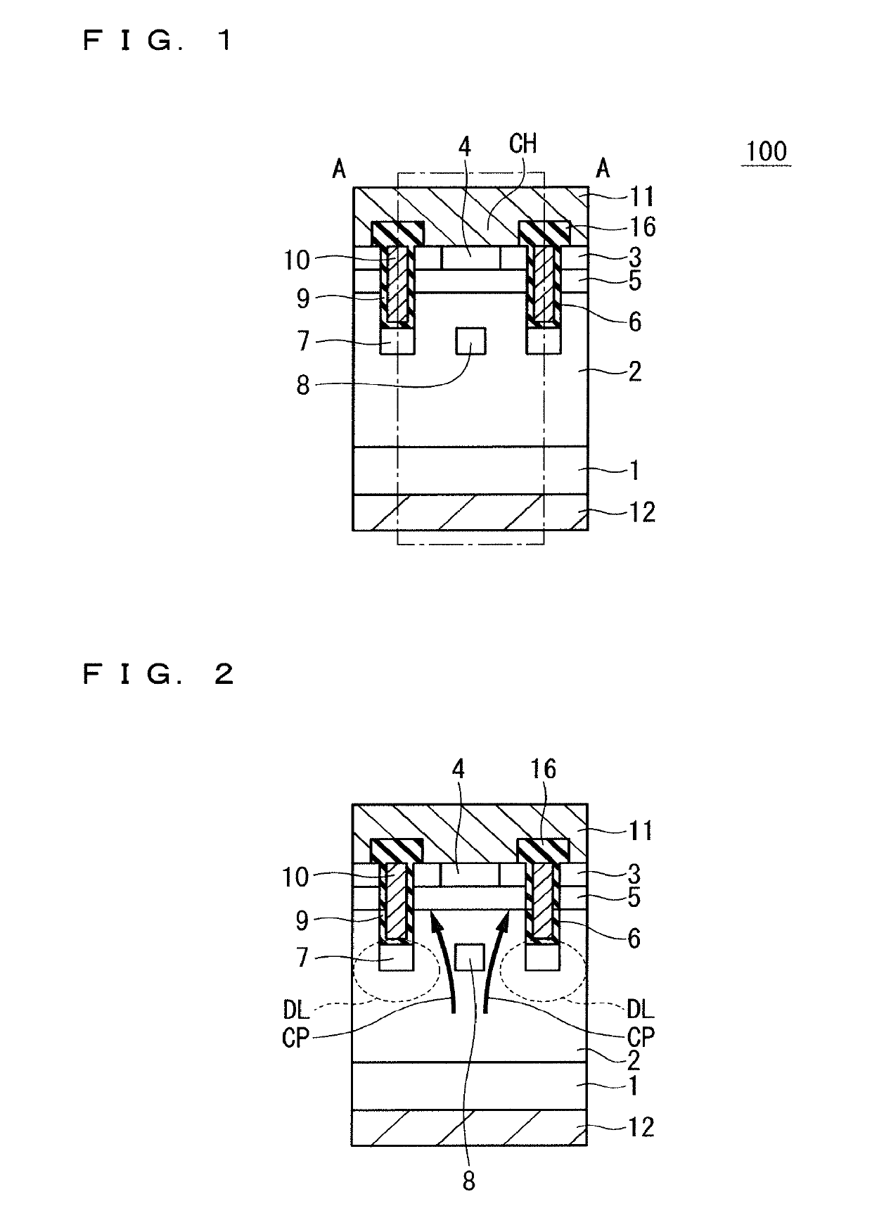
[0061]FIG. 1 is a sectional view schematically showing a partial configuration of a field effect transistor (SiC-MOSFET) 100 having a MOS structure formed on a SiC substrate. In FIG. 1, the minimum unit structure of the MOS, which is called “cell”, is shown enclosed by broken lines, and the actual SiC-MOSFET 100 includes a plurality of cells.

[0062]As shown in FIG. 1, the SiC-MOSFET 100 is formed on a SiC substrate 1 containing n-type (first conductivity type) impurities at a relatively high concentration in the range of 1×10¹⁸ to 1×1021 cm−3.

[0063]On the main surface of the SiC substrate 1, a drift layer 2 (semiconductor layer) containing n-type impurities at a relatively low concentration in the range of 1×10¹⁴ to 1×1017 cm−3 is formed. The drift layer 2 is formed by epitaxial growth, for example.

[0064]In an upper layer portion of the drift layer 2, a source region 3 (first semiconductor region) containing n-type impurities (donor impurities) of approximately 1×1019 cm−3 is d...

second embodiment

[0132]FIG. 26 is a sectional view schematically showing a partial configuration of a SiC-MOSFET 200 formed on the SiC substrate. In FIG. 26, the same components as those of the SiC-MOSFET 100 described with reference to FIG. 1 are denoted by the same reference numerals, and repeated descriptions are omitted.

[0133]As shown in FIG. 26, in the SiC-MOSFET 200, the depletion suppressing layer 8 provided in the drift layer 2 between the adjacent trench-bottom protecting layers 7 includes an intermediate point that is horizontally equidistant to the adjacent trench-bottom protecting layer 7, and the depletion suppressing layer 8 is provided at such a position that a distance d1 to a side wall 61 of one of the trenches 6 is different from a distance d2 to a side wall 62 of the other trench 6. That is, the depletion suppressing layer 8 is provided so as to be offset toward one of the trenches 6. Note that the horizontal position of the depletion suppressing layer 8 between the adjacent trenc...

third embodiment

[0142]FIG. 31 is a sectional view schematically showing a partial configuration of a SiC-MOSFET 300 formed on the SiC substrate. In FIG. 30, the same components as those of the SiC-MOSFET 100 described with reference to FIG. 1 are denoted by the same reference numerals, and repeated descriptions are omitted.

[0143]As shown in FIG. 30, in the SiC-MOSFET 300, it is configured such that the depletion suppressing layer 8 provided in the drift layer 2 between the adjacent trench-bottom protecting layers 7 includes a breakdown-voltage sustaining layer 19 containing p-type impurities in the horizontally central part.

[0144]With such a configuration adopted, the breakdown-voltage sustaining layer 19 can be caused to also share the electric field during the off-state applied to the trench-bottom protecting layer 7, and it is possible to reduce the field intensity both at the bottom of the body region 5 and the bottom of the trench 6 and to sustain the breakdown voltage.

[0145]That is, when the ...


PUM


Abstract

A semiconductor device including: a trench gate; a trench-bottom protecting layer of a second conductivity type provided in a semiconductor layer of a first conductivity type while contacting a bottom of trenches; and a depletion suppressing layer of the first conductivity type provided between adjacent trench-bottom protecting layers, wherein the depletion suppressing layer includes an intermediate point that is horizontally equidistant to the adjacent trench-bottom protecting layers and is formed of a size to contact neither the trenches nor the trench-bottom protecting layers, and an impurity concentration of the depletion suppressing layer is set higher than an impurity concentration of the semiconductor layer.

Description

TECHNICAL FIELD[0001]The present invention relates to a semiconductor device, and particularly relates to a semiconductor device including a trench gate.BACKGROUND ART[0002]In power electronics equipment, a switching device called an insulated gate semiconductor device such as an IGBT (Insulated Gate Bipolar Transistor) and a[0003]MOSFET (Metal-Oxide-Semiconductor Field Effect Transistor) is widely used to control power supply to a load such as an electric motor.[0004]One example of such an insulated gate semiconductor device is a trench gate type MOSFET in which a gate electrode is embedded in a semiconductor layer. In the trench gate type MOSFET, by forming trenches in the semiconductor layer and using the side surfaces thereof as a channel region, it is possible to increase a channel width density and improve the performance of the device.[0005]Here, as a next generation semiconductor device capable of achieving a high breakdown voltage and a low loss, a semiconductor device (wid...

Claims


Application Information

Patent Timeline
Patent Type & Authority Applications(United States)
IPC IPC(8): H01L29/06H01L29/78H01L29/10H02M7/5387H02M1/08
CPCH01L29/0623H01L29/7813H01L29/1095H02M7/53871H02M1/08H02P27/08H01L29/66068H01L29/66734H01L29/0878H01L29/1608H01L29/0696H01L29/045H01L29/78H01L29/12
Inventor ADACHI, KOHEISUGAWARA, KATSUTOSHIFUKUI, YUTAKATANAKA, RINAKONISHI, KAZUYA
Owner MITSUBISHI ELECTRIC CORP
Why Eureka
Try Eureka