Metal organic chemical vapor depostion (MOCVD) tunnel junction growth in iii-nitride devices

Active Publication Date: 2019-08-08
KING ABDULAZIZ CITY FOR SCIENCE AND TECHNOLOGY +1
View PDF4 Cites 3 Cited by
  • Summary
  • Abstract
  • Description
  • Claims
  • Application Information

AI Technical Summary

Benefits of technology

[0009]The present disclosure describes a structure for improving the performan

Problems solved by technology

Although these materials are standard TCO for LEDs and widely used, they suffer from high optical losses which limits the performance of III-nitride based optoelectronics devices.
However, tunnel junctions grown by MOCVD are difficult to achieve because the grown Mg-dope

Method used


Image

  • Metal organic chemical vapor depostion (MOCVD) tunnel junction growth in iii-nitride devices
  • Metal organic chemical vapor depostion (MOCVD) tunnel junction growth in iii-nitride devices
  • Metal organic chemical vapor depostion (MOCVD) tunnel junction growth in iii-nitride devices

Examples


first embodiment

A. Delta Doping for MOCVD Tunnel Junction Growth in III-Nitride Devices

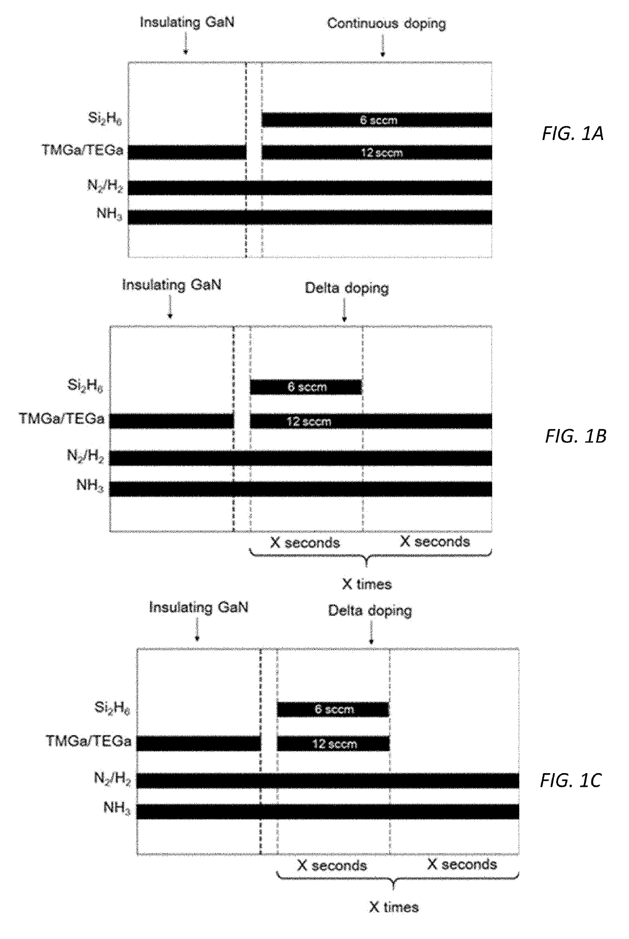
[0053]1. Introduction

[0054]Metal-organic chemical vapor deposition (MOCVD), also referred to as organometallic vapor phase epitaxy (OMVPE) is a type of chemical vapor deposition (CVD) method used to form thin films of various materials and microstructures. This is achieved by flowing volatile organometallic gaseous precursors over a homoepitaxial or heteroepitaxial substrate at elevated temperatures, leading to the growth of high quality (e.g., single) crystal films of various compound semiconductors.

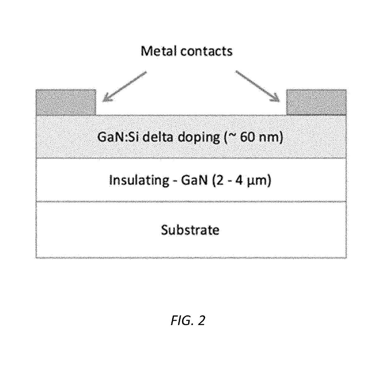
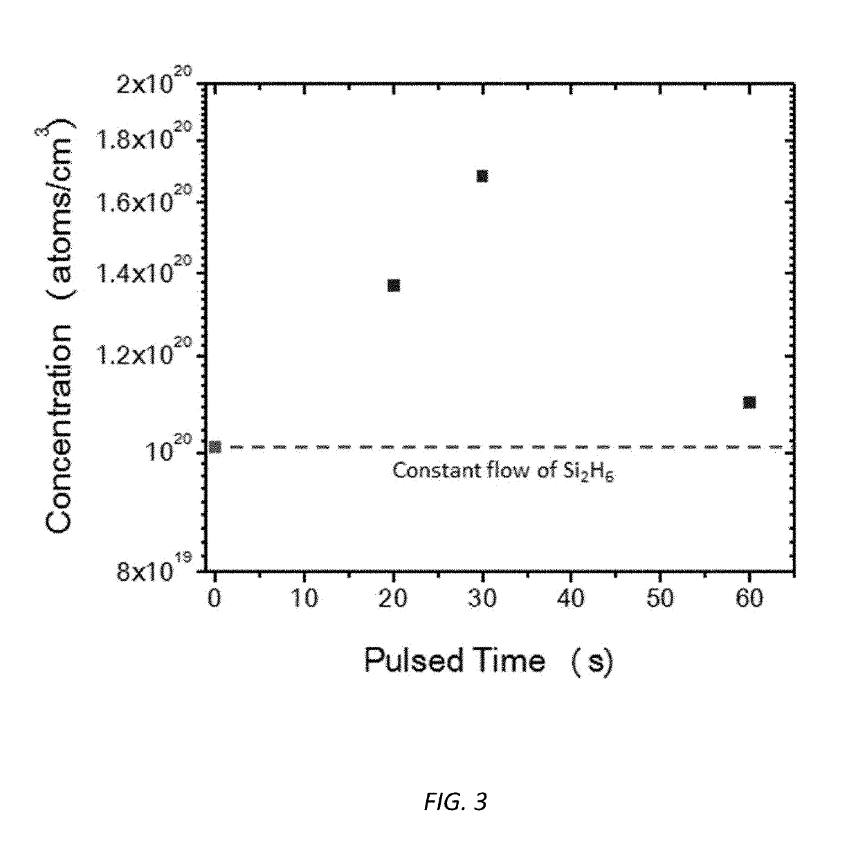
[0055]N-type doping in III-nitride materials can be accomplished by incorporating atoms that act as electron donors, i.e. they have an energy level that sits very close to the conduction band of the host material. To date, optoelectronic devices such as LEDs and LDs have been fabricated with silicon (Si) semiconductor materials. However, heavy Si doping leads to dislocation inclines, resulting in a buildup of tensil...

second embodiment

B. Realization of MOCVD Tunnel Junction Contacts in Large Area III-Nitride Devices

[0083]1. Introduction

[0084]This section describes a regrowth method for large III-nitride (III-N) tunnel junction devices that uses MOCVD to grow light-emitting and / or light-absorbing structures and MOCVD regrowth to grow tunnel junctions.

[0085]P-type GaN is a highly resistive material formed by doping GaN films with Mg.

[0086]Since MOCVD reactions take place at elevated temperatures in the presence of hydrogen gas, charge carrying holes become compensated by the presence of hydrogen-magnesium complexes. In order to activate the holes, these complexes must be dissociated through a high temperature anneal [4]. In addition, carrier concentrations are only a few percent relative to dopant concentrations due to the high activation energy of Mg relative to the valence band edge of III-nitrides. The relatively low hole concentrations make forming low resistance ohmic contacts to p-GaN challenging. N-type dop...


PUM

PropertyMeasurementUnit
Temperatureaaaaaaaaaa
Timeaaaaaaaaaa
Poweraaaaaaaaaa

Abstract

A method for fabricating an (Al,Ga,In,B)N or III-nitride semiconductor device, including performing a growth of III-nitride or (Al,Ga,In,B)N material including a p-n junction with an active region and using metal-organic chemical vapor deposition (MOCVD) or chemical vapor deposition; and performing a subsequent regrowth of n-type (Al,Ga,In,B)N or III-nitride material using MOCVD or chemical vapor deposition while utilizing a pulsed delta n-type doping scheme to realize an abrupt, smoother surface of the n-type material and a higher carrier concentration in the n-type material. In another example, the method comprises forming a mesa having a top surface; and activating magnesium in the p-type GaN of the (Al,Ga,In,B)N material through openings in the top surface that expose the p-type GaN's surface. The openings are formed before or after the subsequent regrowth of the tunnel junction.

Description

CROSS REFERENCE TO RELATED APPLICATIONS[0001]This application claims the benefit under 35 U.S.C. Section 119(e) of the following co-pending and commonly-assigned U.S. applications:[0002]U.S. Provisional Patent Application No. 62 / 627,316, filed Feb. 7, 2018, by Abdullah Ibrahim Alhassan and Steven P DenBaars, entitled “DELTA DOPING FOR MOCVD TUNNEL JUNCTION GROWTH IN III-NITRIDE DEVICES,” Attorney's Docket No. 30794.670-US-P1 (2018-260); and[0003]U.S. Provisional Patent Application No. 62 / 627,312, filed Feb. 7, 2018, by Abdullah Ibrahim Alhassan and Steven P DenBaars, entitled “REALIZATION OF MOCVD TUNNEL JUNCTION CONTACTS IN LARGE AREA III-NITRIDE DEVICES,” Attorney's Docket No. 30794.671-US-P1 (2018-261);[0004]both of which applications are incorporated by reference herein.BACKGROUND OF THE INVENTION1. Field of the Invention[0005]The present invention relates to a method of fabricating tunnel junction devices.2. Description of the Related Art[0006]III-nitride LEDs are a commerciall...

Claims


Application Information

Patent Timeline
IPC IPC(8): H01L33/00H01L33/32H01L33/06
CPCH01L33/0075H01L33/325H01L33/06C23C16/18C23C16/34H01L33/40H01L33/32H01L33/38H01L2933/0083C30B29/406C30B25/04C30B25/02
Inventor ALHASSAN, ABDULLAH IBRAHIMSPECK, JAMES S.DENBAARS, STEVEN P.
Owner KING ABDULAZIZ CITY FOR SCIENCE AND TECHNOLOGY
Why Eureka
Try Eureka