Organic electroluminescent compound and organic electroluminescent device comprising the same
- Summary
- Abstract
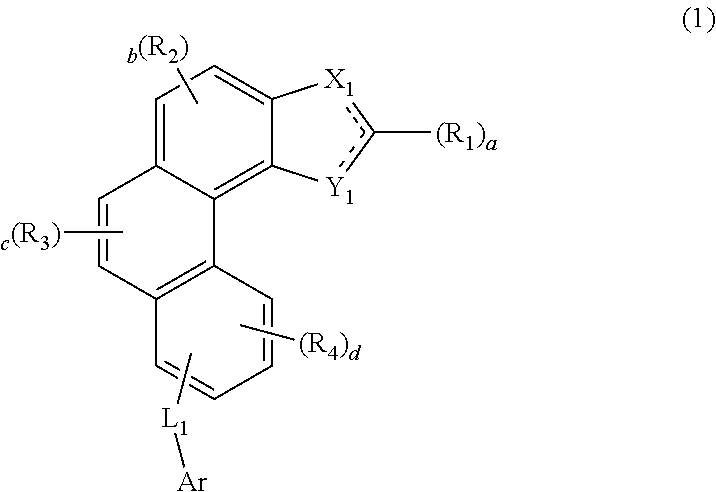
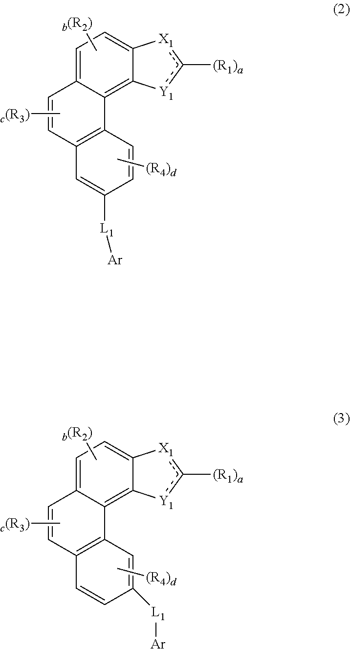
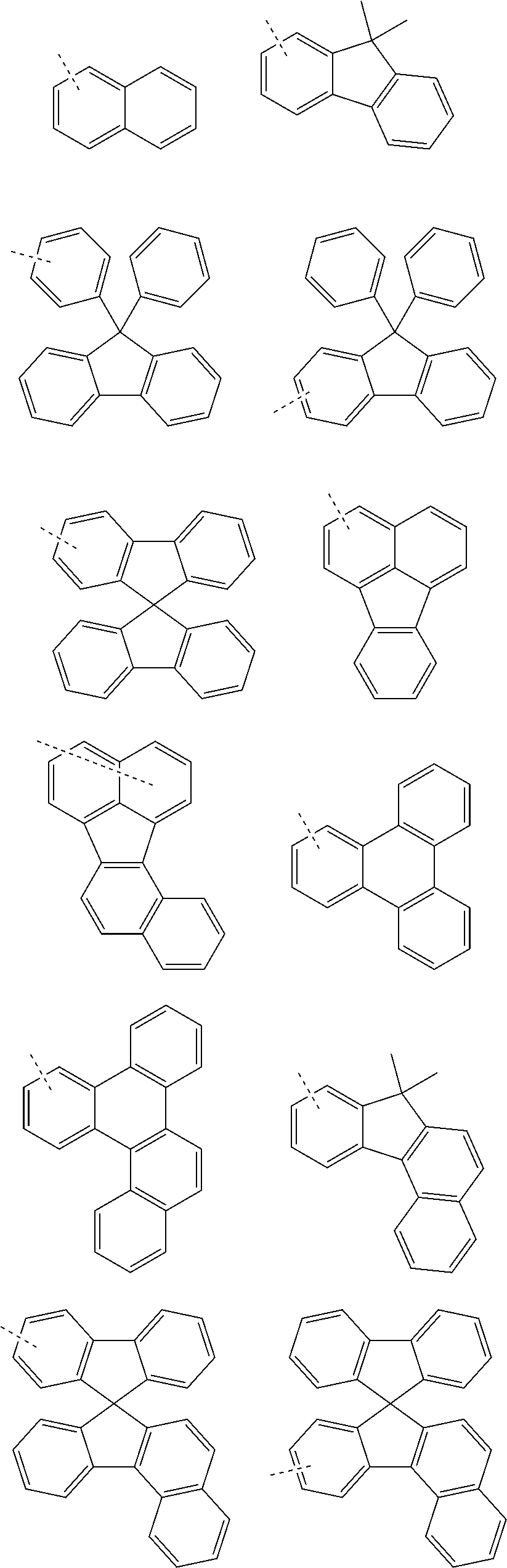
- Description
- Claims
- Application Information
AI Technical Summary
Benefits of technology
Problems solved by technology
Method used
Image

Examples
example 2
on of Compound C-24
[0063]
[0064]Compound A (3.3 g, 8 mmol), 2-(3-bromophenyl)triphenylene (3 g, 8 mmol), tetrakis(triphenylphosphine)palladium (0.3 g, 0.3 mmol), potassium carbonate (2.7 g, 20 mmol), 40 mL of toluene, 10 mL of ethanol, and 10 mL of distilled water were added into a reaction vessel and stirred at 120° C. for 3 hours. After completion of the reaction, the organic layer mixture was washed with distilled water and extracted with ethyl acetate. The extracted organic layer was dried with magnesium sulfate and the solvent was removed by a rotary evaporator. Thereafter, the residue was purified by column chromatography to obtain the compound C-24 (2.5 g, yield: 53%).
MWUVPLM.P.C-24597.72395 nm481 nm287° C.
example 3
on of Compound 1-4
[0065]
[0066]1) Preparation of Compound 1-1
[0067]Compound B (CAS: 1044146-16-8, 36 g, 124 mmol), 4-chloro-2-formylbenzeneboronic acid (25.2 g, 136 mmol), tetrakis(triphenylphosphine)palladium (5.7 g, 5.0 mmol), sodium carbonate (33 g, 150 mmol), 600 mL of toluene, 150 mL of ethanol, and 150 mL of distilled water were added into a reaction vessel and stirred at 140° C. for 3 hours. After completion of the reaction, the precipitated solid was washed with distilled water and methanol. The obtained compound 1-1 was used in the next reaction without further purification.
[0068]2) Preparation of Compound 1-2
[0069]Compound 1-1 (45.6 g, 130 mmol), (methoxymethyl)triphenylphosphonium chloride (74.3 g, 217 mmol), and 1,500 mL of tetrahydrofuran were added into a reaction vessel and the reaction mixture was stirred for 5 minutes. Potassium t-butoxide (1 M in THF, 220 mL) was then slowly added dropwise at 0° C. The temperature was slowly raised and the reaction mixture was stirr...
example 1
[Device Example 1] Producing a Blue Light-Emitting Organic Electroluminescent Device According to the Present Disclosure
[0077]An OLED device was produced in the same manner as in Comparative Example 1, except that compound C-23 as an electron buffer material having a thickness of 5 nm was deposited on the light-emitting layer to form an electron buffer layer, and compound ETL-1 and compound EIL-1 were deposited in a weight ratio of 50:50 to form an electron transport layer of 30 nm on the electron buffer layer.
[0078]The results of the driving voltage, the luminous efficiency, and the color coordinates of the organic electroluminescent device of Comparative Example 1 and Device Example 1 produced as described above at a luminance of 1,000 nits are shown in the following Table 1.
TABLE 1ElectronDrivingLuminousColorColorBufferVoltageEfficiencyCoordinateCoordinateMaterial(V)(cd / A)(x)(y)Comparative—3.85.90.1390.092Example 1Device Example 1C-233.66.60.1390.091
[Comparative Example 2] Produc...
PUM
 Abstract
Description
Claims
Application Information
 - R&D
- Intellectual Property
- Life Sciences
- Materials
- Tech Scout
- Unparalleled Data Quality
- Higher Quality Content
- 60% Fewer Hallucinations
Browse by: Latest US Patents, China's latest patents, Technical Efficacy Thesaurus, Application Domain, Technology Topic, Popular Technical Reports.
© 2025 PatSnap. All rights reserved.Legal|Privacy policy|Modern Slavery Act Transparency Statement|Sitemap|About US| Contact US: help@patsnap.com