Dynamic random access memory structure and method for preparing the same

a random access memory and dynamic technology, applied in nanoinformatics, instruments, transistors, etc., can solve the problems of affecting the formation of capacitors, and reducing the size of the bottom electrode, so as to achieve superior stiffness and strength, and increase the length-to-diameter

Active Publication Date: 2020-01-23
NAN YA TECH
View PDF4 Cites 6 Cited by
  • Summary
  • Abstract
  • Description
  • Claims
  • Application Information

AI Technical Summary

Benefits of technology

[0024]In the present disclosure, each carbon nanotube has a diameter in nanometer scale, and it is therefore easy to form the plurality of carbon nanotubes on the landing pad, even when a width or a length of the landing pad is less than 10 nm. Further, the carbon nanotube has a larger length-to-diameter ratio, which can be up to 132,000,000:1, and superior stiffness and strength even with such large length-to-diameter ratio. Therefore, each of the plurality of carbon nanotubes, which serve as a bottom electrode of a capacitor in a DRAM cell structure, has a very large surface area. Accordingly, capacitance of the capacitor is high. In addition, during the forming of the bottom electrode, the plurality of carbon nanotubes can be grown vertically and can be separated from each other without extra photolithography and etching processes, simplifying the manufacturing process, and improving both yield and reliability of the manufacturing process.
[0025]In contrast, with a comparative method applied without forming the plurality of carbon nanotubes, photolithography and etching processes are required to form at least one bottom electrode over the drain region. It is difficult to form such bottom electrode with a length-to-diameter ratio as large as that of the present disclosure, and thus formation of a thick conductive layer may be required, and followed by the photolithography and etching processes described above. Such processes are complicated. Further, it is observed that a bottom electrode, even one with a length-to-diameter ratio less than that of the carbon nanotubes, may collapse. Accordingly, the conventional processes for forming DRAM cell structure are not only complicated, but also provide reduced yield and reliability.

Problems solved by technology

However, when the critical dimension of a DRAM cell structure is reduced to sub-20 nm scale, the occupied area is too small to allow formation of a capacitor with a very tall, vertical cylinder shape using current photolithography and etching processes.
Such processes are complicated.
Further, it is observed that a bottom electrode, even one with a length-to-diameter ratio less than that of the carbon nanotubes, may collapse.
Accordingly, the conventional processes for forming DRAM cell structure are not only complicated, but also provide reduced yield and reliability.

Method used


Image

  • Dynamic random access memory structure and method for preparing the same
  • Dynamic random access memory structure and method for preparing the same
  • Dynamic random access memory structure and method for preparing the same

Examples


first embodiment

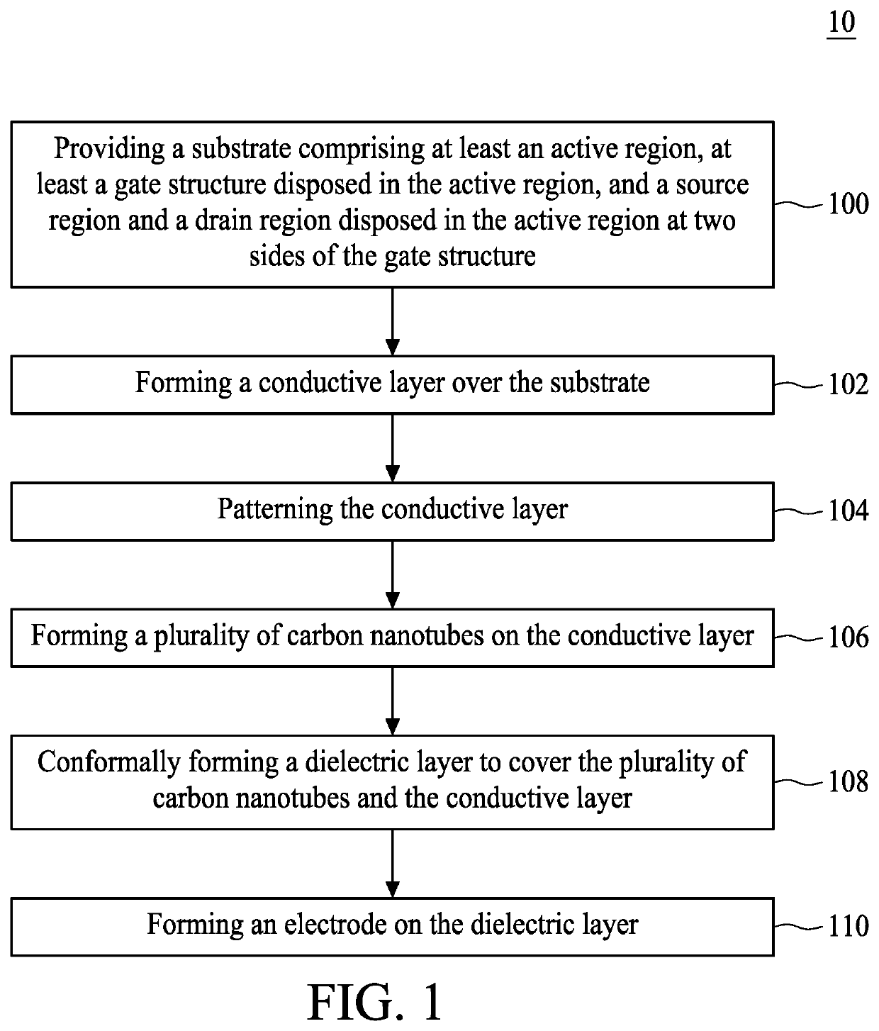
[0039]FIG. 1 is a flow diagram illustrating a method for preparing a DRAM cell structure in accordance with the present disclosure. The method for preparing the DRAM cell structure 10 includes a step 100, providing a substrate. The substrate can include at least an active region, at least a gate structure disposed in the active region, and a source region and a drain region disposed in the active region at two sides of the gate structure. The method for preparing the DRAM cell structure 10 further includes a step 102, forming a conductive layer over the substrate. The method for preparing the DRAM cell structure 10 further includes a step 104, patterning the conductive layer. The method for preparing the DRAM cell structure 10 further includes a step 106, forming a plurality of carbon nanotubes on the conductive layer. The method for preparing the DRAM cell structure 10 further includes a step 108, conformally forming a dielectric layer to cover the plurality of carbon nanotubes and...

second embodiment

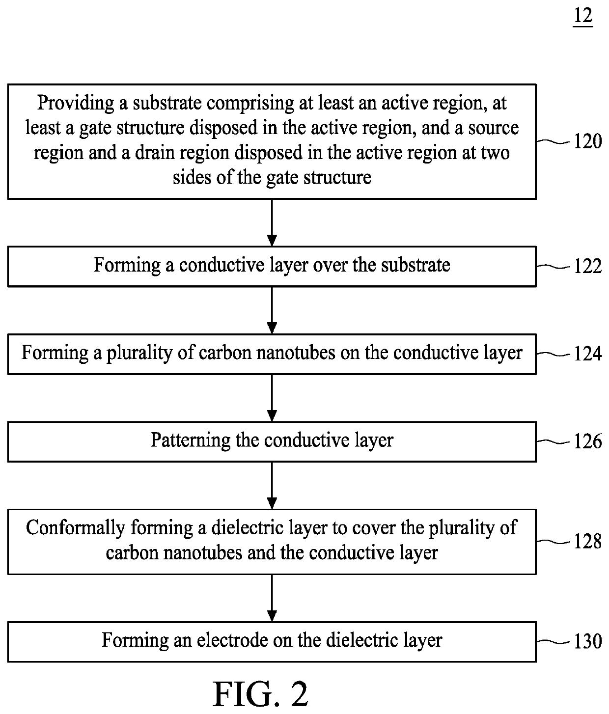
[0040]FIG. 2 is a flow diagram illustrating a method for preparing a DRAM cell structure in accordance with the present disclosure. The method for preparing the DRAM cell structure 12 includes a step 120, providing a substrate. The substrate can include at least an active region, at least a gate structure disposed in the active region, and a source region and a drain region disposed in the active region at two sides of the gate structure. The method for preparing the DRAM cell structure 12 further includes a step 122, forming a conductive layer over the substrate. The method for preparing the DRAM cell structure 12 further includes a step 124, forming a plurality of carbon nanotubes on the conductive layer. The method for preparing the DRAM cell structure 12 further includes a step 126, patterning the conductive layer. The method for preparing the DRAM cell structure 12 further includes a step 128, conformally forming a dielectric layer to cover the plurality of carbon nanotubes and...


PUM

PropertyMeasurementUnit
lengthaaaaaaaaaa
diameteraaaaaaaaaa
diameteraaaaaaaaaa

Abstract

The present disclosure provides a DRAM cell structure. The DRAM cell structure includes a substrate, a gate structure disposed in the substrate, a source region and a drain region disposed in the substrate respectively at two sides of the gate structure, a landing pad disposed over the drain region, a plurality of carbon nanotubes disposed on the landing pad, a top electrode disposed over the plurality of carbon nanotubes, and a dielectric layer disposed between the top electrode and the plurality of carbon nanotubes.

Description

TECHNICAL FIELD[0001]The present disclosure relates to a dynamic random access memory (DRAM) structure and a method for preparing the same, and more particularly, to a capacitor in a DRAM cell structure and a method for preparing the same.DISCUSSION OF THE BACKGROUND[0002]A DRAM cell structure typically includes a metal-oxide-semiconductor field effect transistor (MOSFET) device and a capacitor that are built in or on a semiconductor silicon substrate. The MOSFET device and the capacitor form a series connection with each other. Using a word line and a bit line, a DRAM cell structure can be read and programmed.[0003]There is a continuing trend of increasing the storage density of integrated circuit memories to provide increased quantities of data storage on a single chip. To address the challenges of reduced structure sizes, DRAM designs have been proposed which incorporate capacitors having vertical extensions above the surface of the substrate (“stacked” capacitors) or below the s...

Claims


Application Information

Patent Timeline
Patent Type & Authority Applications(United States)
IPC IPC(8): H01L27/108G11C13/02G11C11/401
CPCH01L27/108H01L27/10855B82Y40/00H01L27/10885B82Y30/00H01L27/10805G11C11/401G11C13/025B82Y10/00H10B12/318H10B12/34H10B12/315H10B12/48H10B12/0335H01L28/90H10B12/00H10B12/30H10B12/482
Inventor CHUANG, DA-ZENSUN, CHIH-CHUNG
Owner NAN YA TECH
Why Eureka
Try Eureka