A magnetometer using optically active defects in a solid state material

a solid-state material, optically active technology, applied in the direction of magnetic field measurement using magneto-optic devices, optical pumping analysis, electron paramagnetic resonance analysis, etc., can solve the problems of only achieving high-sensitivity magnetometers, limited application to particular processes, etc., to achieve the same level of sensitivity, high efficiency, and enhanced efficiency of fluorescence light generation

Active Publication Date: 2020-05-21
DANMARKS TEKNISKE UNIV
View PDF0 Cites 8 Cited by
  • Summary
  • Abstract
  • Description
  • Claims
  • Application Information

AI Technical Summary

Benefits of technology

[0020]The invention is particularly, but not exclusively, advantageous for obtaining a magnetometer, which has enhanced efficiency and responsivity of fluorescence light generation facilitated by the particular integration and use of the optical cavity and RF / microwave coupling structure, e.g. via a resonant antenna. Specifically, the high efficiency relates to the fact that to obtain the same level of sensitivity conventionally (e.g. without the use of the optical cavity), at least an order of magnitude larger power of irradiation laser for excitation, e.g. green laser light, is required.
[0021]Another advantage as compared to for example Jensen et al. mentioned above is that the present invention can be implemented with one only irradiation laser for excitation of the paramagnetic defects, whereas the Jensen et al. setup requires two laser source, one for pumping the optical cavity and one for probing.
[0022]The magnetometer of the present invention may therefore have direct applications in fields ranging from sub-surface geophysical exploration, to biomedical sensing and imaging of magnetically active processes / specimens (both ex- and in-situ) due to its ease of handling, non-toxicity, and low optical power consumption compared to competing technologies available.

Problems solved by technology

Their application is also limited to particular processes at a time as they are only capably of sensing within narrow frequency bandwidths, in environments that will not degrade their electronic functionality.
Apart from diamond-based magnetometers, high sensitivity magnetometers (with pico- to femto-Tesla sensitivities) are only achieved with atomic vapor cells and superconducting interference devices.
Atomic vapor is toxic, and while it is enclosed in a glass cell, it may only find limited use in a clinical setting due to safety reasons.
In addition, superconducting devices require cryogenic temperatures making them extremely expensive and limited in their applicability.
However, to reach the needed sensitivity for such measurements, the concentration of NV centers has hitherto been increased artificially and / or the optical collection efficiency has been increased by more advanced optical configurations, both factors leading to more complex or relatively costly measuring configurations of the ODMR based magnetometers.
However, this study suggests further nitrogen vacancy centers to be positioned in the artificial diamond, which is complicated and expensive in itself, and increasing the NV concentration may also cause various optical saturations effects, thus this magnetometer configuration for ODMR has certain shortcomings for increasing the sensitivity.
Furthermore, this technique requires at least two lasers, one for pumping and one for probing the absorption making it more difficult to perform miniaturization.

Method used


Image

  • A magnetometer using optically active defects in a solid state material
  • A magnetometer using optically active defects in a solid state material
  • A magnetometer using optically active defects in a solid state material

Examples


Embodiment Construction

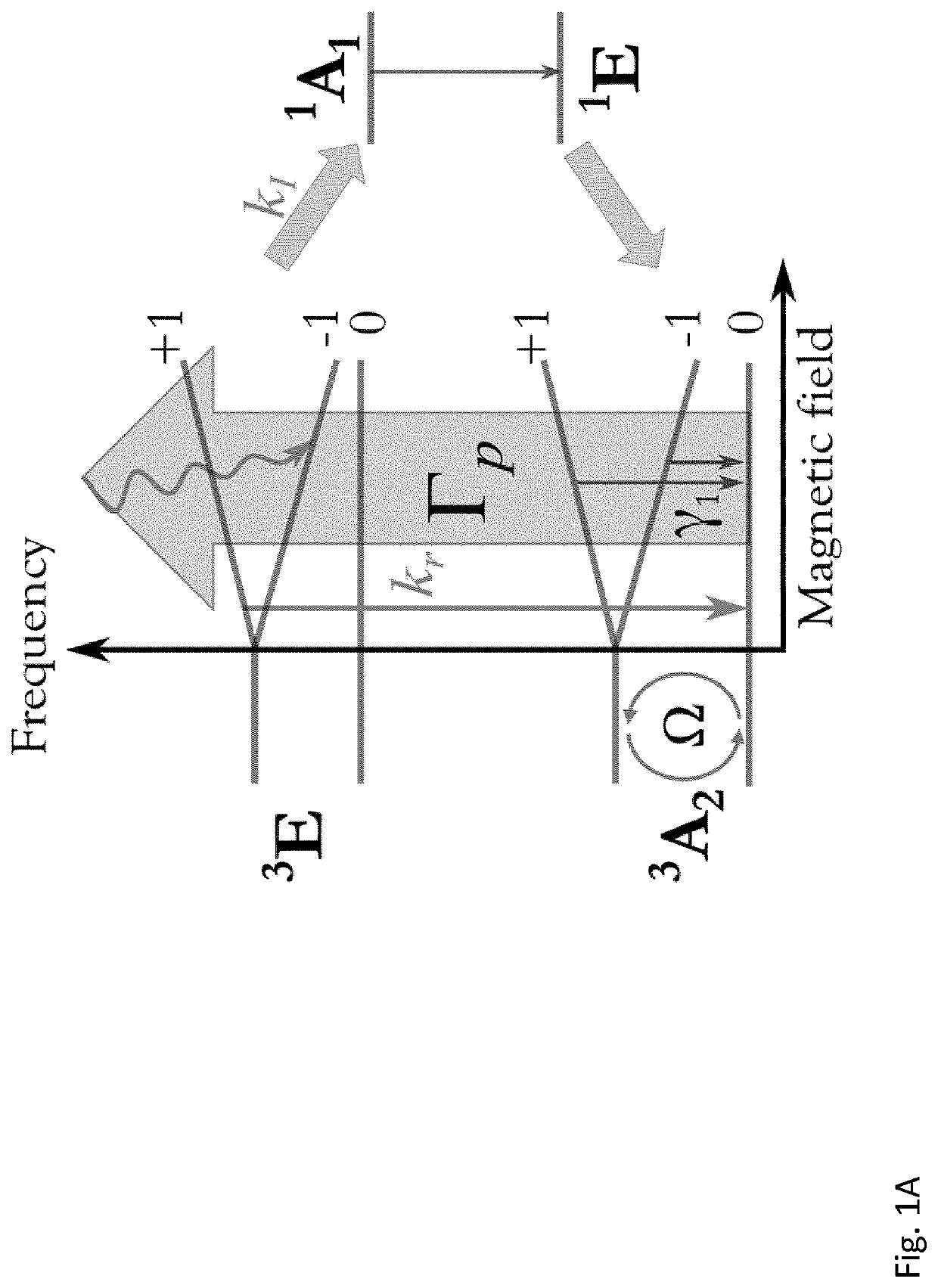
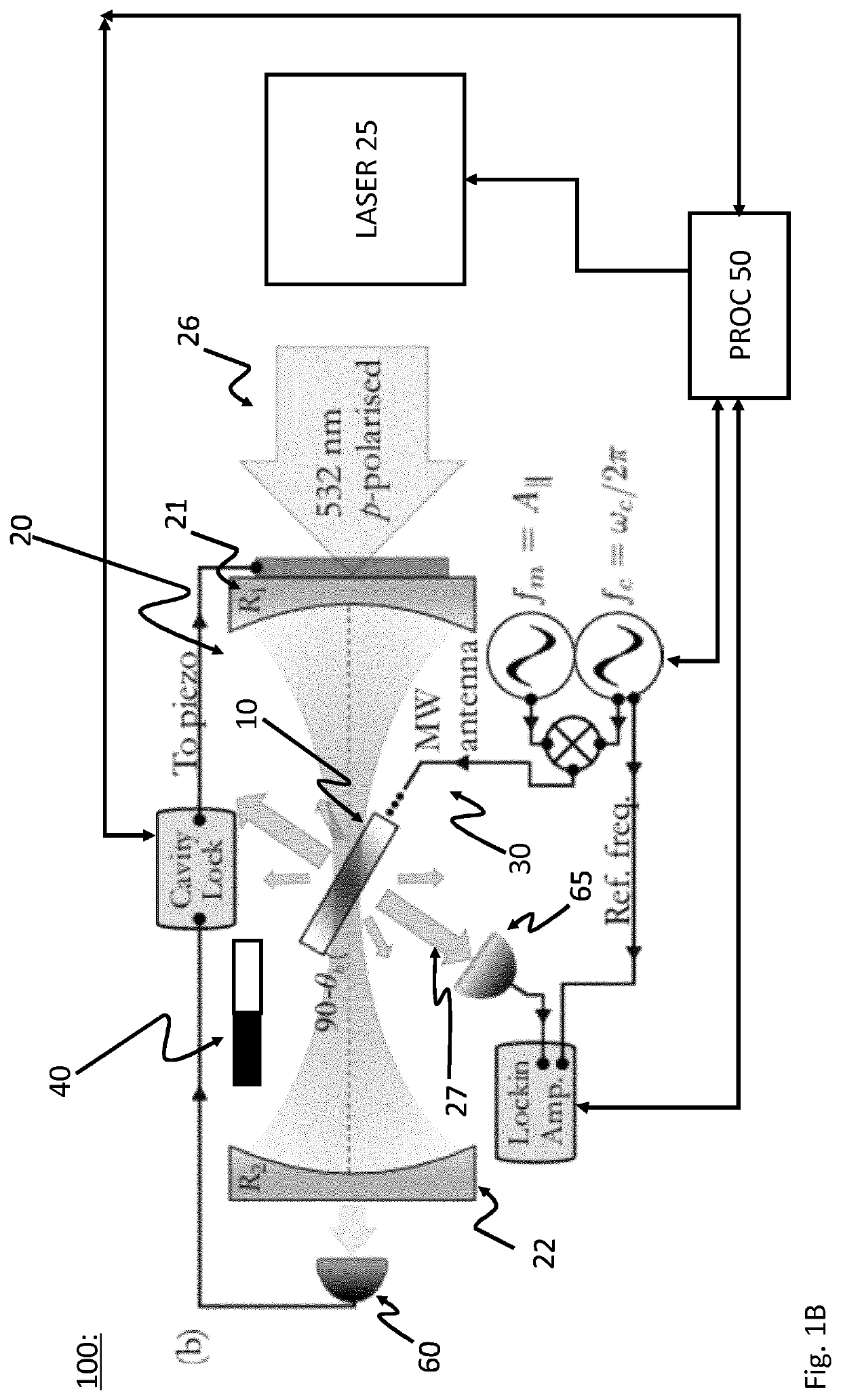
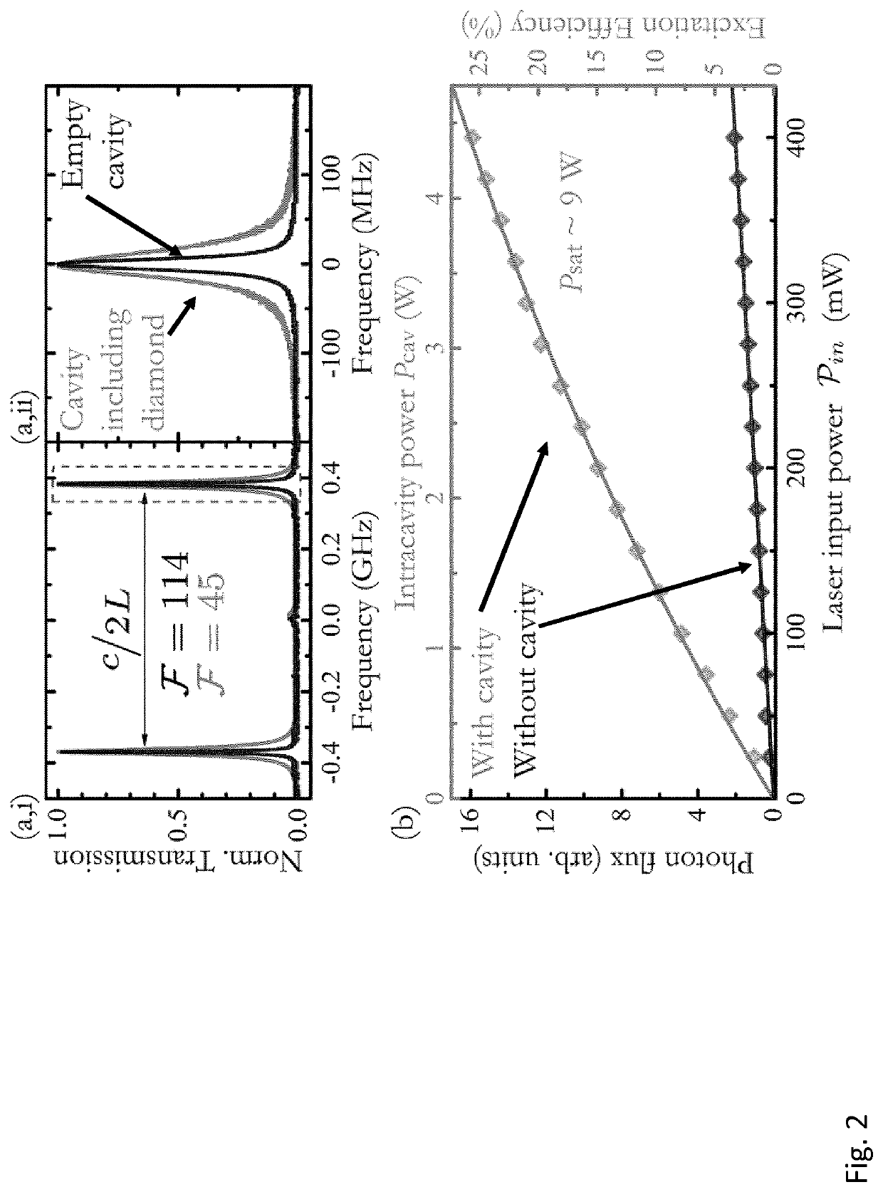
[0064]FIG. 1A is an energy diagram of the NV defects in diamond, where the electronic configuration of the NV center (schematic shown in FIG. 1(a)) exhibits spin-dependent fluorescence by virtue of the difference between the ms=±1 and the ms=0 spin levels inter-system crossing rates (kI) from the 3E excited triplet state to the shelving singlet states (1A1-1E). In a simplifed continuous wave (cw) picture for an ensemble of identical systems, the radiative relaxation rate (kr) of all the excited state levels competes with kI to bring about a fluorescence contrast (C) based on the initial distribution of the spinstate population in the triplet ground states (3A2). This ground state spin population is set by the ratio between the optical read-out pump rate Γp from above-band excitation (in this case a 532 nm laser), and the resonant microwave (MW) drive rate of the spin levels (Rabi frequency Ω), of which the optical above-band excitation mechanisms is near-perfect spin conserving. The...


PUM

PropertyMeasurementUnit
external magnetic fieldaaaaaaaaaa
optically detected magnetic resonanceaaaaaaaaaa
magnetic fieldaaaaaaaaaa

Abstract

The present invention relates to a magnetometer (100) using optically detected magnetic resonance (ODMR), where a solid state material (10), such as diamond, with an ensemble of paramagnetic defects, such as nitrogen vacancies centers NV, is applied. An optical cavity (20) is optically excited by an irradiation laser (25) arranged therefore. A coupling structure (30) causes a microwave excitation (Ω) of the paramagnetic defects, and a permanent magnetic field (40, B_C) causes a Zeeman splitting of the energy levels in the paramagnetic defects. A probing volume (PV) in the solid state material is thereby defined by the spatially overlapping volume of the optical excitation by the irradiation laser (25), the coupling structure (30) also exciting the defects, and the constant magnetic field. The magnetometer then measures an unknown magnetic field by detecting emission (27), e.g. fluorescence, from the defects in the probing volume (PV) from the double excitation of the defects by the irradiation laser, and the coupling structure exciting these defects.

Description

FIELD OF THE INVENTION[0001]The present invention relates to a magnetometer for measuring a magnetic field using optically active defects in a solid state material, such as a crystal diamond with nitrogen-vacancies centers or defects, and a corresponding method for measuring such magnetic fields.BACKGROUND OF THE INVENTION[0002]Conventional magnetometer products consist of MEMS-based microchips with sensitivities scaling down towards the 10 nano-Tesla / Hz{circumflex over ( )}(1 / 2) level, which limits their applicability to sensing large fields such as those stemming from geomagnetic processes, or electro / magneto-electronics. Their application is also limited to particular processes at a time as they are only capably of sensing within narrow frequency bandwidths, in environments that will not degrade their electronic functionality.[0003]Apart from diamond-based magnetometers, high sensitivity magnetometers (with pico- to femto-Tesla sensitivities) are only achieved with atomic vapor c...

Claims


Application Information

Patent Timeline
Patent Type & Authority Applications(United States)
IPC IPC(8): G01R33/32G01R33/032G01N24/00
CPCG01N24/006G01R33/323G01R33/032G01N24/10G01R33/26G01R33/60
Inventor HUCK, ALEXANDERAHMADI, SEPEHREL-ELLA, HAITHAM A. R.ANDERSEN, ULRIK LUND
Owner DANMARKS TEKNISKE UNIV
Why Eureka
Try Eureka