Electroluminescent device, and display device comprising thereof

Active Publication Date: 2021-04-08
SAMSUNG ELECTRONICS CO LTD
View PDF0 Cites 1 Cited by
  • Summary
  • Abstract
  • Description
  • Claims
  • Application Information

AI Technical Summary

Benefits of technology

[0028]An electroluminescent device having improved life-span and/or luminous

Problems solved by technology

Particularly, in order to improve the quantum efficiency, excitons may be confined in the light emitting layer, but when the e

Method used


Image

  • Electroluminescent device, and display device comprising thereof
  • Electroluminescent device, and display device comprising thereof
  • Electroluminescent device, and display device comprising thereof

Examples


Example

Verification Example 1

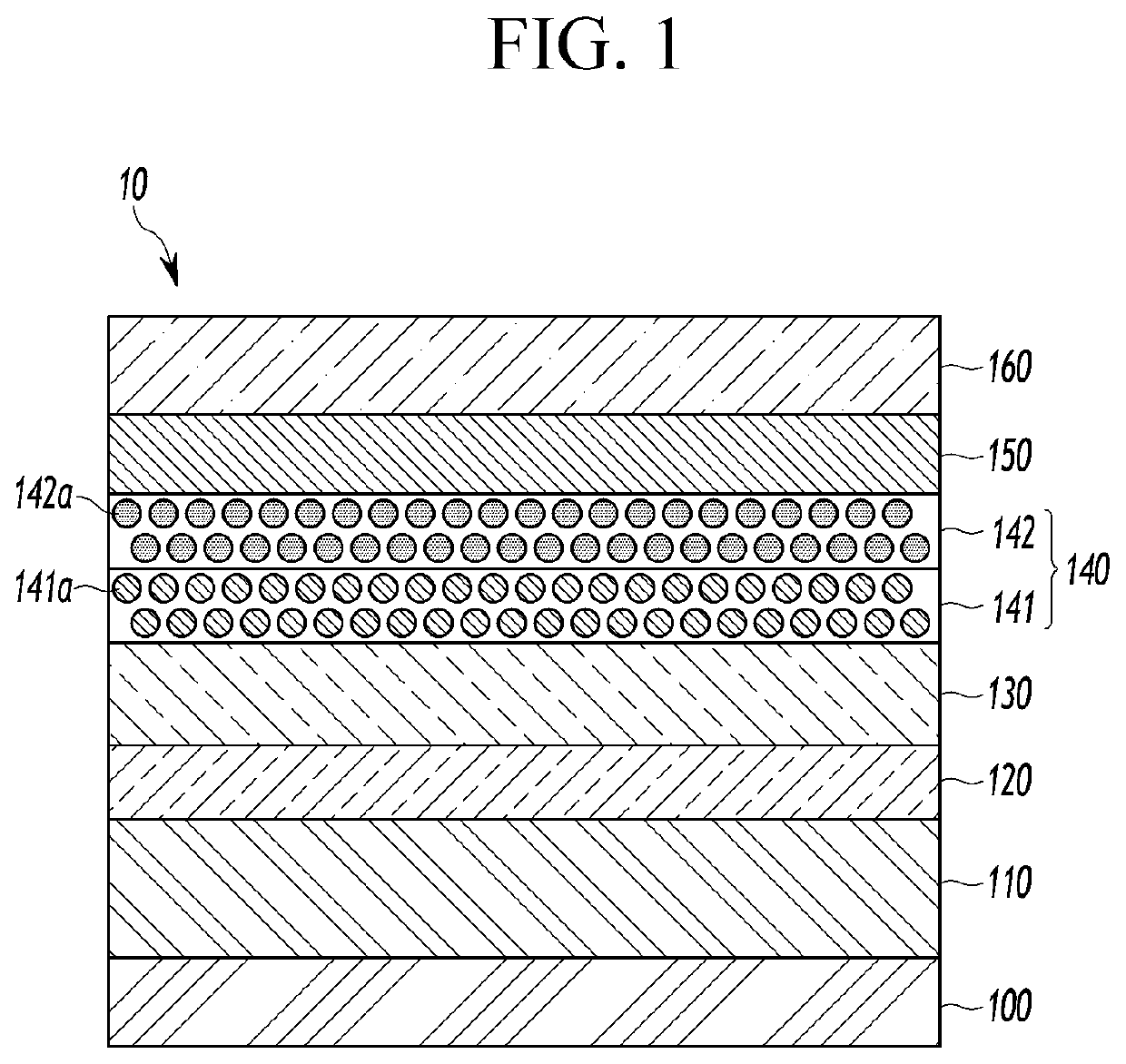
[0184]A glass substrate deposited with ITO as a first electrode (an anode) is surface-treated with UV-ozone for 15 minutes, and a PEDOT: PSS solution (HOMO energy level: −5.35 eV, HC Starks) is spin-coated thereon and heat-treated 150° C. for 30 minutes under a nitrogen atmosphere to form a 30 nm-thick hole injection layer. Here, HOMO stands for highest occupied molecular orbital.

[0185]On the hole injection layer (TFB, an HOMO energy level: −5.56 eV, a LUMO energy level: −2.69 eV, Sumitomo Co., Ltd.), a solution prepared by dissolving poly[(9,9-dioctylfluorenyl-2,7-diyl-co(4,4′-(N-4-butylphenyl) diphenylamine] in o-xylene is spin-coated and heat-treated at 150° C. for 30 minutes to form a 25 nm-thick first hole transport layer. Here, LUMO stands for lowest unoccupied molecular orbital.

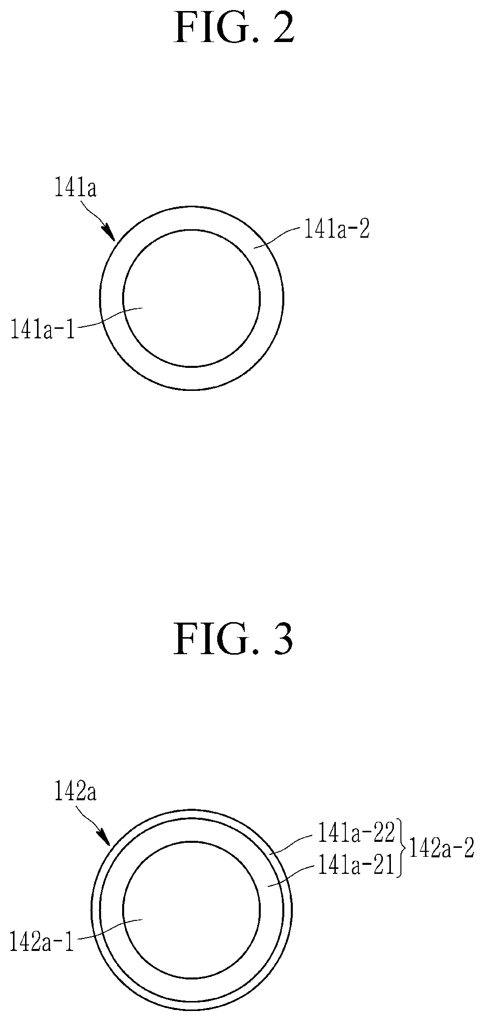
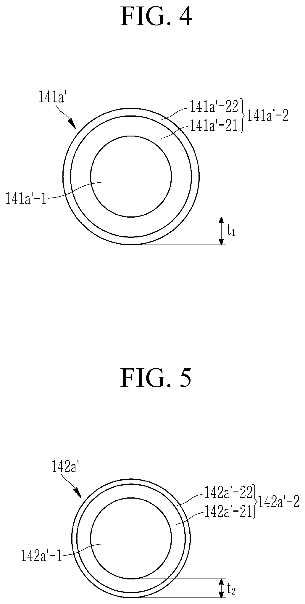
[0186]Subsequently, a composition for a light emitting layer, which is prepared by dispersing an InP / ZnSe core-single shell quantum dot to which oleate as a hydrophobic ligand is ...

Example

Verification Example 2

[0190]HOD (Hole Only Device) according to Verification Example 2 (ITO / PEDOT:PSS / TFB / Red QD (InP / ZnSe / ZnS) / GSH0137 / HAT-CN / Ag) is produced according to the same method as Verification Example 1 except that an InP / ZnSe / ZnS core-double shell quantum dot to which oleate as a hydrophobic ligand is attached (an average particle diameter: 18 nm, a peak emission wavelength: 630 nm) is used instead of the InP / ZnSe core-single shell quantum dot to which oleate as a hydrophobic ligand is attached.

Example

Verification Example 3

[0191]An ITO-deposited glass substrate as a first electrode (an anode) is surface-treated with UV-ozone for 15 minutes, and a solution for an electron transport layer, which is prepared by dispersing ZnMgO (an average particle diameter: 2 nm to 5 nm) in ethanol, is spin-coated thereon and heat-treated at 80° C. for 30 minutes to form a 20 nm-thick first electron transport layer.

[0192]Subsequently, a composition for a light emitting layer, which is prepared by dispersing an InP / ZnSe core-single shell quantum dot to which oleate as a hydrophobic ligand is attached (an average particle diameter: 18 nm, a peak emission wavelength: 630 nm) in octane, is spin-coated and heat-treated at 80° C. to form a 20 nm-thick (red) light emitting layer.

[0193]On the light emitting layer, a solution for an electron transport layer, which is prepared by dispersing ZnMgO (average particle diameter: 2 nm to 5 nm) in ethanol, is spin-coated and heat-treated at 80° C. for 30 minutes to...


PUM

PropertyMeasurementUnit
Thicknessaaaaaaaaaa
Thicknessaaaaaaaaaa
Thicknessaaaaaaaaaa

Abstract

An electroluminescent device includes a first electrode and a second electrode facing each other; a hole transport layer between the first electrode and the second electrode; a light emitting layer including a first light emitting layer disposed between the hole transport layer and the second electrode and including a first quantum dot and a second light emitting layer between the first light emitting layer and the second electrode and including a second quantum dot; and an electron transport layer between the light emitting layer and the second electrode. Each of the first and second light emitting layers emits first light, each of the first and second quantum dots has a core-shell structure including one or more shells, and the first and second quantum dots have different numbers of shells from each other or have different total thicknesses of the one or more shells from each other.

Description

CROSS-REFERENCE TO RELATED APPLICATION[0001]This application claims priority to Korean Patent Application No. 10-2019-0123994 filed on Oct. 7, 2019, and all the benefits accruing therefrom under 35 U.S.C. § 119, the content of which in its entirety is herein incorporated by reference.BACKGROUND1. Field[0002]An electroluminescent device and a display device comprising thereof are disclosed.2. Description of the Related Art[0003]A quantum dot is a nanocrystal of a semiconductor material with a diameter of several nanometers to several tens of nanometers, which exhibits a quantum confinement effect. The quantum dot generates stronger light in a narrow wavelength region than commonly used phosphors. The quantum dot emits light while excited electron is transited from a conduction band to a valence band, and a wavelength of the emitted light is changed depending upon a particle size of the quantum dot even in the same material. As the quantum dot emits light of a shorter wavelength with ...

Claims


Application Information

Patent Timeline
IPC IPC(8): H01L51/50H01L51/00
CPCH01L51/502H01L51/5056H01L51/0037H01L51/0007H01L51/5072H01L2251/5369H01L2251/558H01L51/0039H10K50/15H10K50/11H10K2102/331Y10S977/774H10K50/115H10K50/13H10K50/16H10K2102/00H10K2102/351H10K85/115H10K85/1135H10K71/15
Inventor PARK, SUJINWON, YUHOJANG, EUN JOOCHUNG, DAE YOUNGKIM, SUNG WOOKIM, JIN A.HAN, YONG SEOK
Owner SAMSUNG ELECTRONICS CO LTD
Why Eureka
Try Eureka