
Eureka
For R&D, Eureka makes reading and utilizing patents & technical documents easy.
Eureka AIR
Designed for self-driven R&D workflows. Generate viable solutions, solve complex R&D challenges, empower your innovation with AI.

Eureka Materials
Designed for material experts only. Revolutionize your material R&D, from search, analyze, to developing new materials.

TechResearch
Generate reliable direction feasibility study reports for your R&D in just a few steps.

TechSeek
Discover and master advanced knowledge NOW. Basics, ideas, possibilities, all at once.

TechMind
As an expert in R&D Theories, TechMind can generates customized viable solutions instantly.

TechRisk
Analyze your overall solution with one click, know your potential R&D risks in advance.

TechMonitor
Get weekly tech updates, stay abreast of the latest tech innovations and key insights.
Hard-mask forming composition, method for manufacturing electronic component, and resin
- Summary
- Abstract
- Description
- Claims
- Application Information
AI Technical Summary
Benefits of technology
Problems solved by technology
Method used
Image

Examples
first embodiment
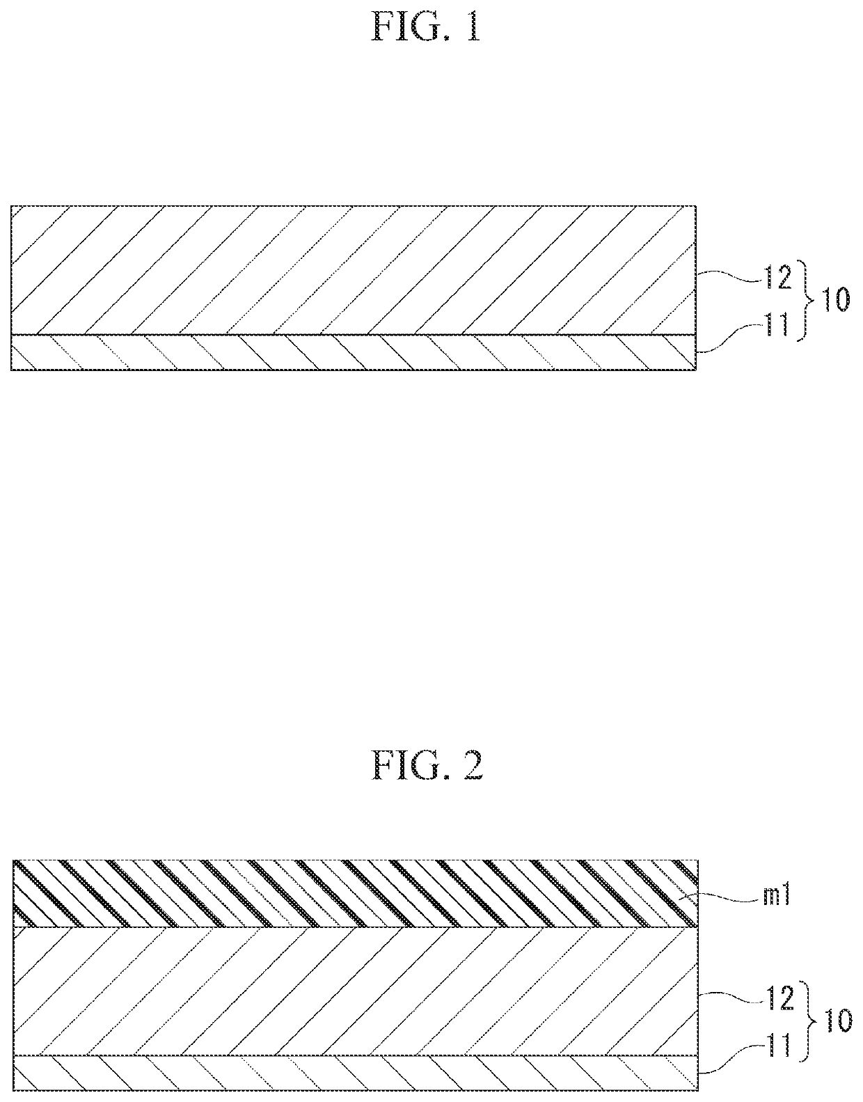
[0219]The method for manufacturing an electronic component of the present embodiment includes: forming a hard mask layer (m1) on a support using the hard-mask forming composition stated above (hereinafter, referred to as “Step (i-i)”); and processing the support using the hard mask layer (m1) as a mask (hereinafter, referred to as “Step (i-a)”).
[0220]FIG. 1 shows a support 10 formed of a substrate 11 and a processing layer 12.
[0221]First, the hard mask layer (m1) is formed on the support 10 using the hard-mask forming composition according to the embodiment stated above (FIG. 2; Step (i-i)).
[0222][Step (i-i)]
[0223]Step (i-i) is a step of forming the hard mask layer (m1) on the support 10 using the hard-mask forming composition according to the embodiment stated above.
[0224]The substrate 11 is not particularly limited and a known substrate in the related art can be used. Examples thereof include a substrate for an electronic component, a substrate on which a predetermined wiring patt...
second embodiment
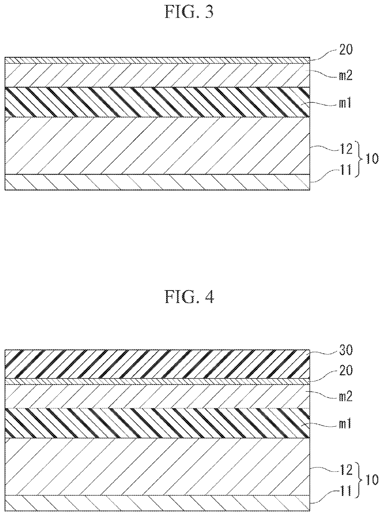
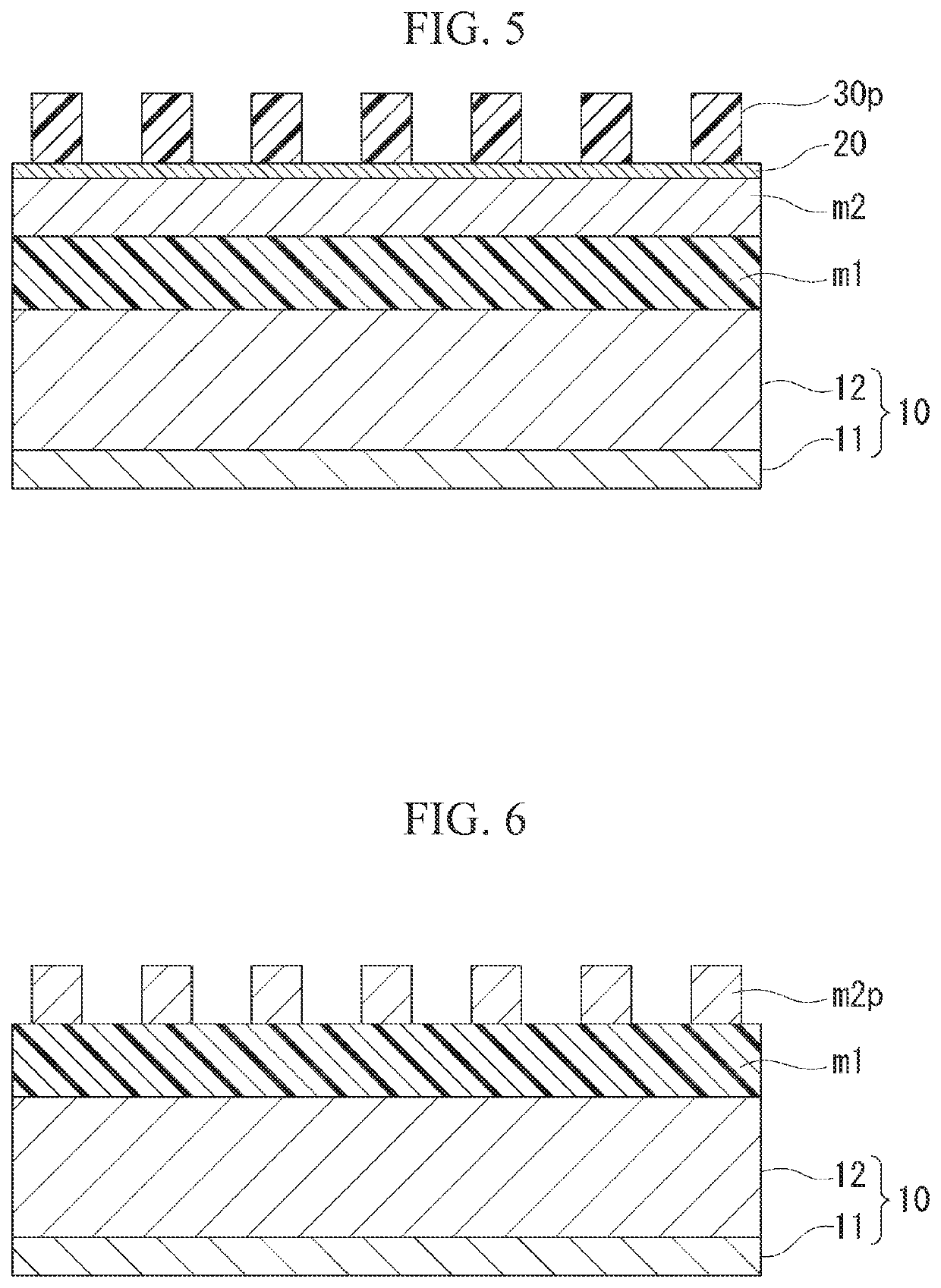
[0231]The method for manufacturing an electronic component of the present embodiment includes:
[0232]forming a hard mask layer (m1) on a support using the hard-mask forming composition according to the embodiment stated above (hereinafter, referred to as “Step (ii-i)”);
[0233]forming a hard mask layer (m2) made of an inorganic material on the hard mask layer (m1) (hereinafter, referred to as “Step (ii-ii)”);
[0234]forming a resist film on the hard mask layer (m2) (hereinafter, referred to as “Step (ii-iii)”);
[0235]forming a resist pattern on the hard mask layer (m2) by exposing the resist film and developing the exposed resist film (hereinafter, referred to as “Step (ii-iv)”);
[0236]etching the hard mask layer (m2) using the resist pattern as a mask to form an inorganic pattern (hereinafter, referred to as “Step (ii-v)”);
[0237]etching the hard mask layer (m1) using the inorganic pattern as a mask to form a resin pattern (hereinafter, referred to as “Step (ii-vi)”); and
[0238]processing t...
third embodiment
[0296]The method for manufacturing an electronic component of the present embodiment includes:
[0297]forming a hard mask layer (m1) on a support using the hard-mask forming composition according to the embodiment stated above (hereinafter, referred to as “Step (iii-i)”);
[0298]forming an inorganic pattern made of an inorganic material on the hard mask layer (m1) (hereinafter, referred to as “Step (iii-v)”);
[0299]etching the hard mask layer (m1) using the inorganic pattern as a mask to form a resin pattern (hereinafter, referred to as “Step (iii-vi)”), and processing the support using the resin pattern as a mask (hereinafter, referred to as “Step (iii-vii)”).
[0300]The method for manufacturing an electronic component according to a fourth aspect is the same as the method for manufacturing an electronic component according to the third aspect, except that the inorganic pattern made of an inorganic material is formed directly on the hard mask layer (m1) without forming a resist film.
[0301...
PUM
| Property | Measurement | Unit |
|---|---|---|
| Fraction | aaaaa | aaaaa |
| Fraction | aaaaa | aaaaa |
| Fraction | aaaaa | aaaaa |
Abstract
Description
Claims
Application Information
 - R&D Engineer
- R&D Manager
- IP Professional
- Industry Leading Data Capabilities
- Powerful AI technology
- Patent DNA Extraction
Browse by: Latest US Patents, China's latest patents, Technical Efficacy Thesaurus, Application Domain, Technology Topic, Popular Technical Reports.
© 2024 PatSnap. All rights reserved.Legal|Privacy policy|Modern Slavery Act Transparency Statement|Sitemap|About US| Contact US: help@patsnap.com