Method of depositing epitaxial material, structure formed using the method, and system for performing the method

a technology of epitaxial material and deposit method, which is applied in the direction of polycrystalline material growth, chemically reactive gas growth, crystal growth process, etc., can solve the problems of time-consuming and expensive cleaning of the reaction chamber after each process run, difficult to remove materials, etc., to achieve the effect of facilitating control of film thickness, composition, other properties, and uniformity

Pending Publication Date: 2021-09-23
ASM IP HLDG BV
View PDF7 Cites 116 Cited by
  • Summary
  • Abstract
  • Description
  • Claims
  • Application Information

AI Technical Summary

Benefits of technology

[0008]In accordance with exemplary embodiments of the disclosure, a method of depositing an epitaxial material layer is provided. The method can be used to form a plurality of epitaxial material layers on a surface of a substrate. Exemplary methods include coating a surface of a reaction chamber with a precoat material, providing a substrate within a reaction chamber of a reactor system (e.g., after the step of coating), depositing one or more epitaxial material layers on a surface of the substrate; and repeating the steps of providing a substrate within a reaction chamber and depositing an epitaxial material layer on the surface of the substrate prior to a step of cleaning the reaction chamber. Exemplary methods can further include the step of cleaning the reaction chamber. Exemplary precoat material includes silicon. The precoat material can include additional elements, such as germanium. In accordance with examples of the disclosure, the precoat material includes greater than 70 atomic percent silicon. In accordance with further examples of the disclosure, a precursor including a halogen is provided to the reaction chamber. Additionally or alternatively, an etchant is provided to the reaction chamber during the step of depositing the epitaxial material layer and/or the step of coating a surface of a reaction chamber with a precoat material. The etchant can include, for example, a halogen. The step of providing a substrate within a reaction chamber can be repeated three or ...

Problems solved by technology

Further, once material deposits onto the walls of the reaction chamber and/or susceptor, the material can be difficult to remove.
Although su...

Method used


Image

  • Method of depositing epitaxial material, structure formed using the method, and system for performing the method
  • Method of depositing epitaxial material, structure formed using the method, and system for performing the method
  • Method of depositing epitaxial material, structure formed using the method, and system for performing the method

Examples


Embodiment Construction

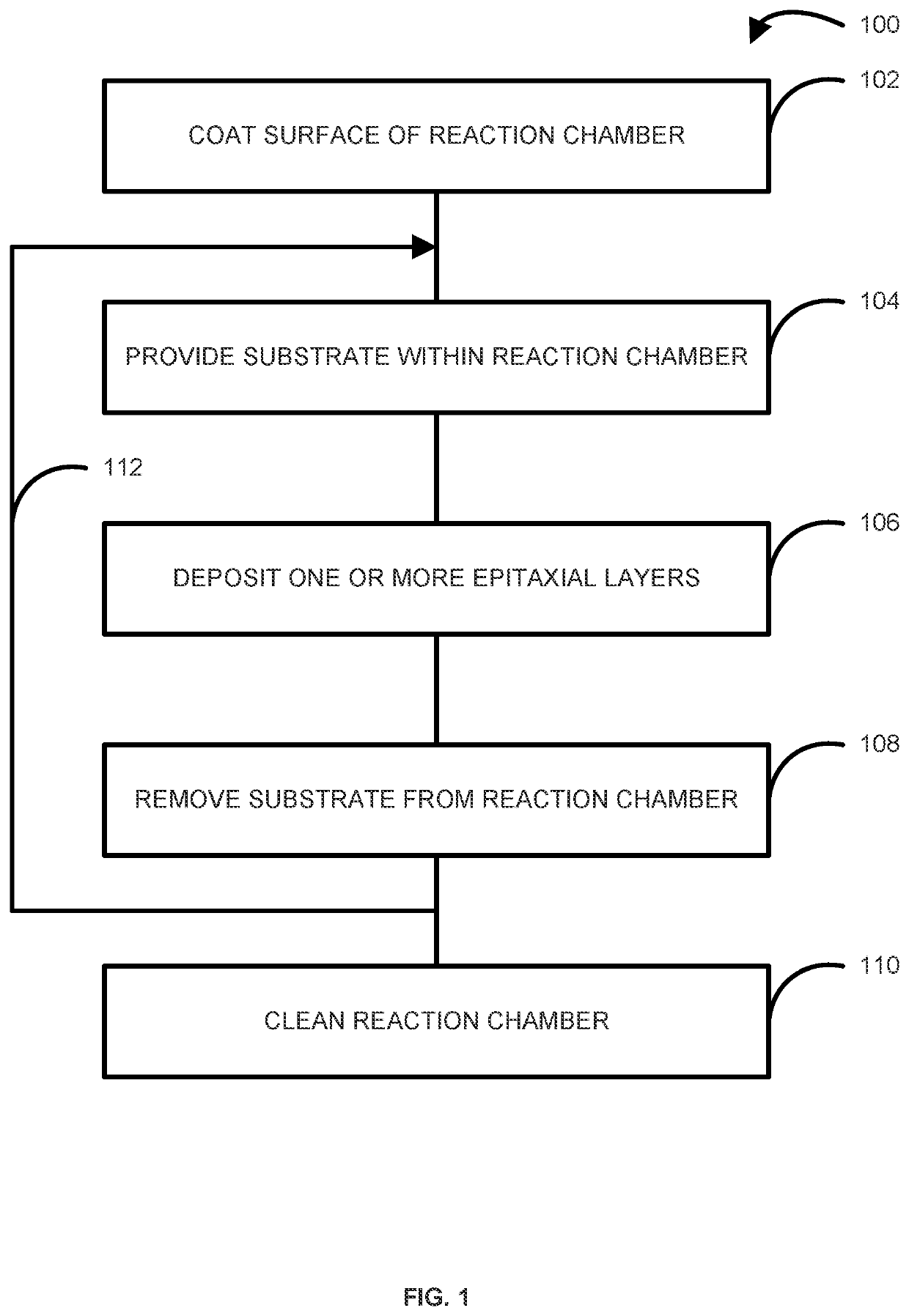
[0020]The description of exemplary embodiments provided below is merely exemplary and is intended for purposes of illustration only; the following description is not intended to limit the scope of the disclosure or the claims. Moreover, recitation of multiple embodiments having stated features is not intended to exclude other embodiments having additional features or other embodiments incorporating different combinations of the stated features.

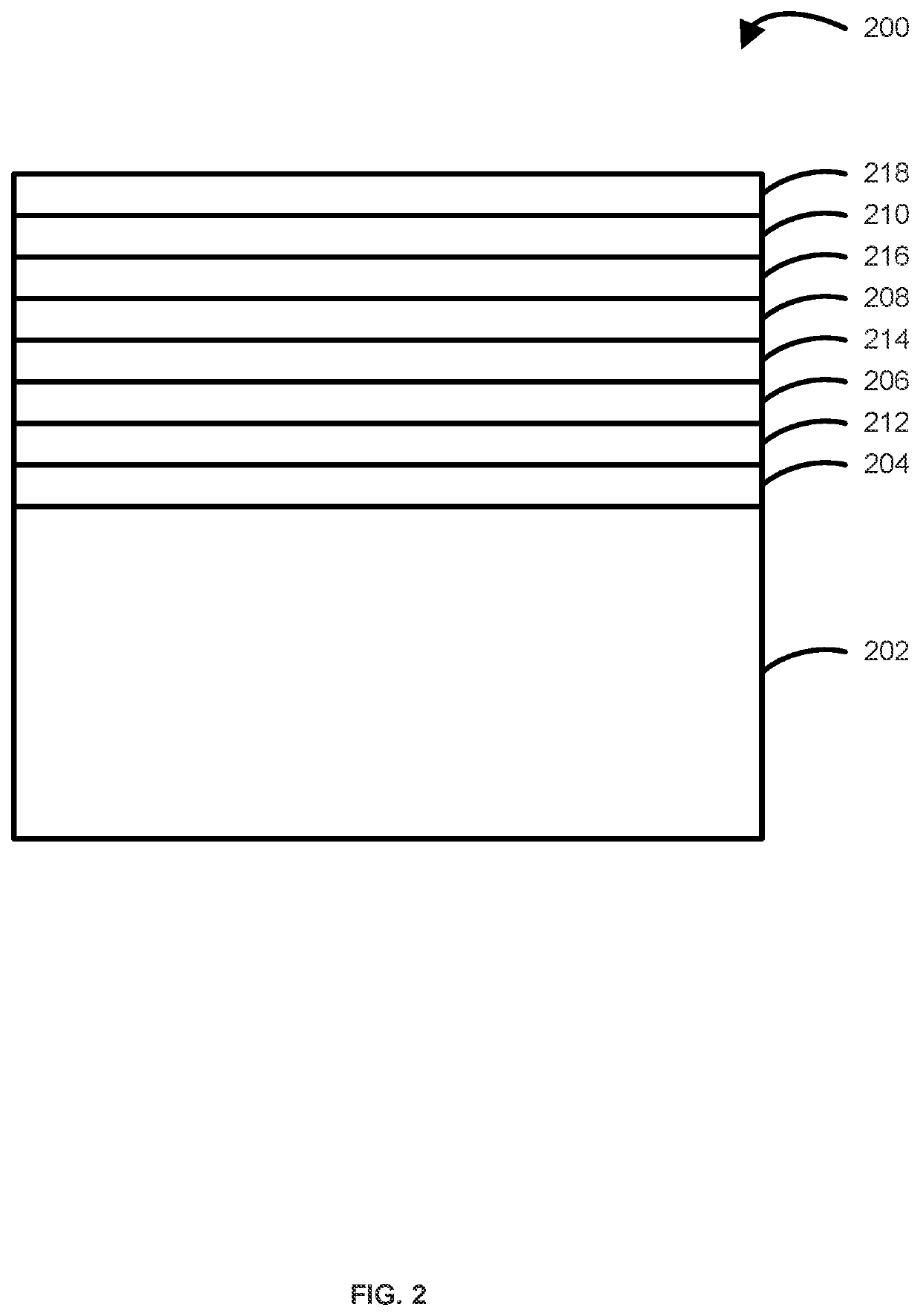
[0021]The present disclosure generally relates to methods and systems for depositing epitaxial material. Exemplary methods and systems can be used to process substrates, such as semiconductor wafers, during the manufacture of devices, such as semiconductor devices, flat panel display devices, photovoltaic devices, microelectromechanical systems (MEMS), and the like. By way of examples, exemplary systems and methods described herein can be used to form or grow epitaxial layers (e.g., one component, two component and / or doped semiconductor layer...


PUM

PropertyMeasurementUnit
Temperatureaaaaaaaaaa

Abstract

A method of depositing one or more epitaxial material layers, a device structure formed using the method and a system for performing the method are disclosed. Exemplary methods include coating a surface of a reaction chamber with a precoat material, processing a number of substrates, and then cleaning the reaction chamber.

Description

CROSS-REFERENCE TO RELATED APPLICATIONS[0001]This application is a nonprovisional of, and claims priority to and the benefit of, U.S. Provisional Patent Application No. 62 / 990,807, filed Mar. 17, 2020 and entitled “METHOD OF DEPOSITING EPITAXIAL MATERIAL, STRUCTURE FORMED USING THE METHOD, AND SYSTEM FOR PERFORMING THE METHOD,” which is hereby incorporated by reference herein.FIELD OF THE DISCLOSURE[0002]The present disclosure generally relates to gas-phase reactors and systems and to methods of using the reactors and systems. More particularly, the disclosure relates to methods of depositing epitaxial material, to systems for depositing the epitaxial material, and to structures formed using the methods and systems.BACKGROUND OF THE DISCLOSURE[0003]Gas-phase reactors, such as chemical vapor deposition (CVD) reactors, can be used for a variety of applications, including depositing and etching materials on a substrate surface. For example, gas-phase reactors can be used to deposit epi...

Claims


Application Information

Patent Timeline
IPC IPC(8): C23C16/455H01L21/02C23C16/52C23C16/44C23C16/24C23C16/42C23C16/56
CPCC23C16/45557H01L21/02381C23C16/52C23C16/4404C23C16/56C23C16/42H01L21/02532H01L21/0262C23C16/45553C23C16/24C23C16/4405C23C16/28C30B25/10C23C16/46H01L21/02576H01L21/02579H01L21/0245H01L21/02507C30B29/52C30B25/16C30B25/08C30B25/14C30B25/165
Inventor KAJBAFVALA, AMIRMISKIN, CALEB
Owner ASM IP HLDG BV
Why Eureka
Try Eureka