
N-co-doped semiconductor substrate.

Pending Publication Date: 2022-03-03
IV WORKS
View PDF0 Cites 0 Cited by
  • Summary
  • Abstract
  • Description
  • Claims
  • Application Information

AI Technical Summary

Benefits of technology

The patent text describes a method for growing a thick layer of GaN using a process called HVPE. The technique has three main advantages: it can make the first layer of GaN thicker without damaging its crystal quality, it can reduce the dislocation density in the GaN by a factor, and it can cause the thick layer of GaN to separate from its starting substrate during growth. The method involves heating the substrate with a mixed atmosphere of nitrogen, ammonia, and hydrogen to form a single-crystal GaN layer. To achieve a minimum thickness of 200 microns, growth needs to continue for several hours. Overall, the technique allows for the production of a thick and resistant layer of GaN that can be easily handled without risking breakage.

Problems solved by technology

Doping can lead to increase the presence of such defects in the crystal lattice.
All these defects generated during growth can induce imperfections in the final wafer (doping heterogeneity and crystal defects, still high dislocation density) which will induce a failure during the fabrication of optoelectronic and / or electronic devices.
However, such a growth rate leads to a high surface density of macro-inclusions and a lower crystal quality.
The method data indicated show that this is clearly an HVPE process with 2D growth and therefore does not provide a solution for 3D growth processes.

Method used


Image

  • N-co-doped semiconductor substrate.
  • N-co-doped semiconductor substrate.
  • N-co-doped semiconductor substrate.

Examples


example embodiments

[0160]In Example 1 (comparative) GaN growth is performed by HVPE on the basis of a substrate as described for example by WO / 03100839A2 according to substrate according to the process described for example by the publication preferably incorporated WO / 03100839A2 in step (iii). The (volume) flow ratio of N2 / (N2+H2) is 0.2. Furthermore, in the present case, the growth temperature is maintained at 930° C. The structure of the growth front FC observed by scanning electron microscope is shown in FIGS. 4a and 4b.

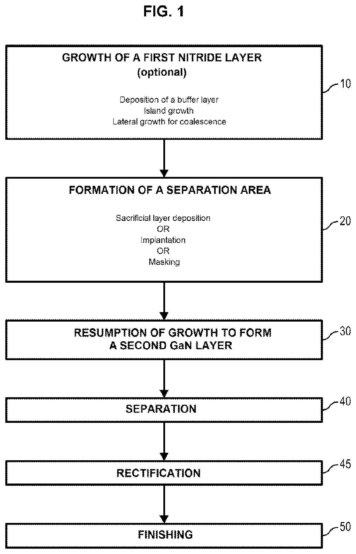
[0161]FIG. 4c depicts the structure of a wafer according to the invention, after grinding and polishing, showing first areas resulting from the growth of non-basal facets with areas resulting from the growth of basal facets.

[0162]In Example 2 (comparative), unlike the previous example, during the HVPE growth phase in step 30 as depicted in FIG. 1, oxygen is introduced in the gas phase (for example 1% O2 diluted in 99% N2 flow sent between 0.2 sccm and 10 sccm) in order to introduc...


PUM


Abstract

A process for fabricating a single-crystal semiconductor material of group 13 nitride, in particular GaN, including the steps of:deposition of at least one single-crystal layer by three-dimensional epitaxial growth on a starting substrate, the layer including areas resulting from the growth of basal facets, and areas resulting from the growth of facets of different orientations, called non-basal facets;supply of an n-dopant gas including a first chemical element selected from the chemical elements of group 16 of the periodic table, and at least one second chemical element selected from the chemical elements of group 14 of the periodic table, such that the concentration of the second element in the areas resulting from the growth of the basal facets is higher than 1.0×10¹⁷ / cm3, and the concentration of the first element in the areas resulting from the growth of the non-basal facets is lower than 2.0×10¹⁸ / cm3.

Description

CROSS-REFERENCE TO RELATED APPLICATIONS[0001]This application is a U.S. national stage of International Application No. PCT / EP2019 / 086123 filed Dec. 18, 2019, which claims the benefit of priority of French Patent Application No. 1873952 filed Dec. 21, 2018, the respective disclosures of which are each incorporated herein by reference in their entireties.FIELD OF THE INVENTION[0002]The invention relates to the general technical field of fabricating substrates and wafers of a semiconductor material based on the elements of columns 13 and 15 of the periodic table—such as gallium nitride GaN.[0003]These wafers are used as substrates for producing semiconductor structures, such as light-emitting diodes (LEDs), laser diodes (LDs), vertical transistors for power electronics, horizontal transistors for power electronics or telecommunications (radio frequency), current rectifier diodes or sensors.BACKGROUND[0004]Current processes for fabricating a semiconductor material substrate based on ni...

Claims


Application Information

Patent Timeline
IPC IPC(8): H01L21/02C30B29/40C30B25/02H01L29/20
CPCH01L21/02389C30B29/403H01L29/2003C30B25/02H01L21/0254H01L21/02378H01L21/0242H01L21/024H01L21/02458H01L21/02576
Inventor BEAUMONT, BERNARDFAURIE, JEAN-PIERREGELLY, VINCENTNAHAS, NABILTENDILLE, FLORIAN
Owner IV WORKS
Learn More