Laser diode device having a substantially circular light output beam and a method of forming a tapered section in a semiconductor device to provide for a reproducible mode profile of the output beam

a laser diode and substantially circular technology, applied in semiconductor lasers, instruments, optical elements, etc., can solve the problems of low fiber coupling efficiency of laser diodes, difficult to precisely control lithographic processes, and difficulty in elliptical laser diode output beam profil

Inactive Publication Date: 2000-04-18
JDS UNIPHASE CORP
View PDF11 Cites 139 Cited by
  • Summary
  • Abstract
  • Description
  • Claims
  • Application Information

AI Technical Summary

Benefits of technology

A further object of this invention is to provide an easier method for fabricating vertical and horizontal waveguide tapers in semiconductor laser devices that provides high reproducibility of the desired mode profile in the output beam from the device.

Problems solved by technology

In particular, low fiber coupling efficiency of laser diodes has been a major limitation for high power single mode fiber output.
This highly divergent, elliptical laser diode output beam profile presents a difficulty when attempting to couple the light from a high power laser diode source to a single mode optical fiber.
This difficulty is primarily due to the large mode mismatch between the semiconductor laser source and the optical fiber.
However, it is difficult to precisely control these lithographic processes and the resultant tapers are not easily reproducible.
However, those techniques require extremely high degree of reproducibility in growth / etch in order to control the beam divergence as desired.
Also, many of the devices fabricated by the conventional techniques in the past suffer from a high degree of optical loss during adiabatic mode conversion.
Further, a significant difficulty with the proposed structure is that the vertical taper continuously extends so that in order to achieve the desired mode profile, the cleaving of the front end facet position becomes critical relative to the exact point of cleave.
Because the dimensions of these devices are in the micron range, it is difficult on a continuous reproducibility basis to form a cleave in a place where the thickness of the waveguide layer will be virtually the same in each case.
This is because the reproducibility of the same identical taper from wafer to wafer is difficult to achieve.
Therefore, there is no guarantee that the desired mode profile will be exactly the same each time or sufficiently optimized to be substantially circular in extent.

Method used


Image

  • Laser diode device having a substantially circular light output beam and a method of forming a tapered section in a semiconductor device to provide for a reproducible mode profile of the output beam
  • Laser diode device having a substantially circular light output beam and a method of forming a tapered section in a semiconductor device to provide for a reproducible mode profile of the output beam
  • Laser diode device having a substantially circular light output beam and a method of forming a tapered section in a semiconductor device to provide for a reproducible mode profile of the output beam

Examples


first embodiment

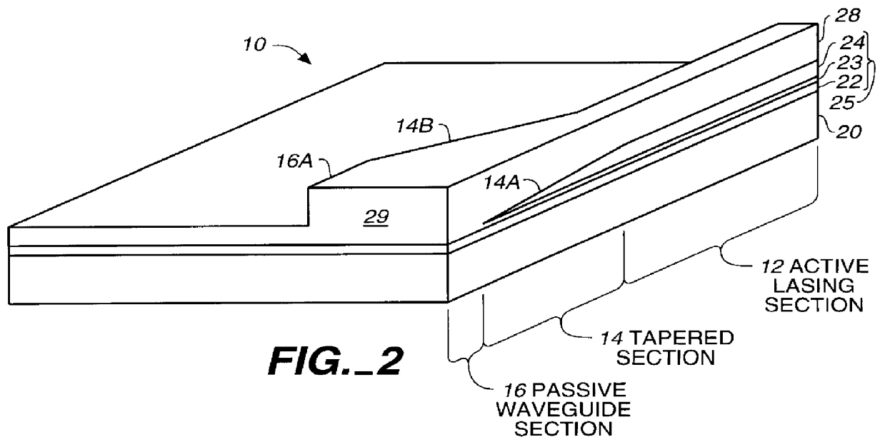
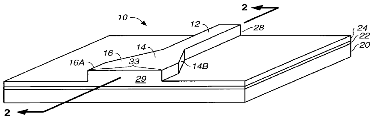
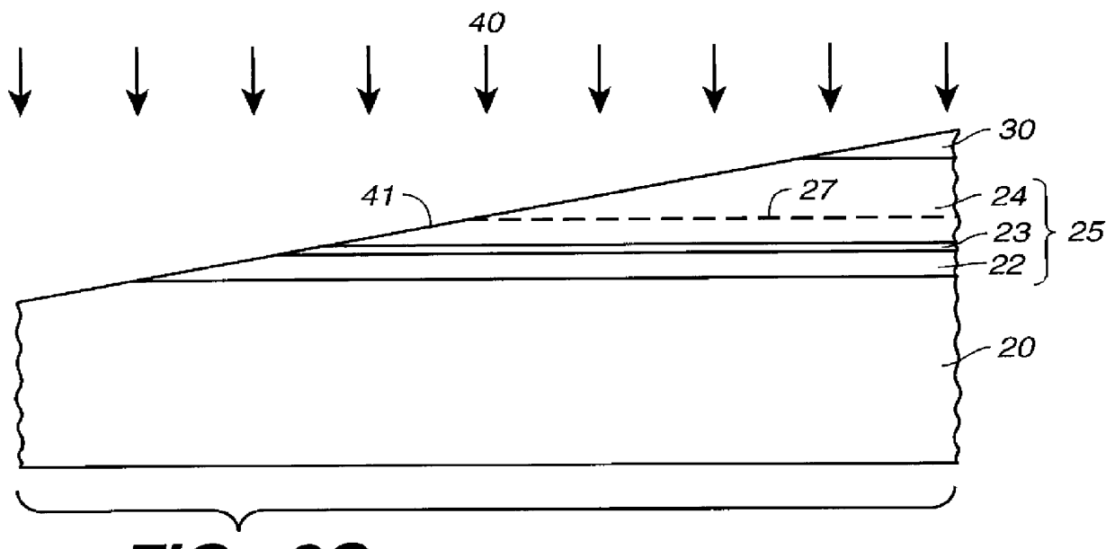
Reference is now made to this invention, illustrated in FIGS. 3A-3D. In the starting base wafer structure, core waveguide structure 25 comprises two waveguide layers 22 and 24, upper layer 24 including an optically active region 27 and lower layer 22 forming a passive waveguide layer. These layers 22 and 24 are 5 separated by a thin InP etch-stop layer 23, e.g., approximately only 200 .ANG. thick. Etch-stop layer 23, being so thin, has no significant detrimental effect to the waveguide properties of the higher index materials comprising layers 22 and 24. Lastly, a sacrificial layer 30 comprising InP is grown on the top of waveguide structure 25. An important factor in achieving the desired mode profile is the determination of the thickness of lower passive waveguide layer 22. Since, as will be described later, layer 22 is left intact via the etching process due to the InP etch-stop layer 23, the resultant expanded profile can be calculated based upon the initial growth thickness est...

second embodiment

Reference is now made to this invention, illustrated in FIGS. 4A-4F which provides for more refined control and reproducibility in the taper etch processing. Instead of a single sacrificial layer 30, in this embodiment a stack of sacrificial layers is employed, for example, a thin etch-stop layer 50 of InP followed by an InGaAsP etch-stop layer 51 which is followed by relatively thick InP sacrificial layer 30. Using this thicker etch-stop layer group 50, 51, a clean surface termination can be achieved after completion of the taper etch step with no remaining sacrificial layer 30. The stack stop-etch layers provide a way to form a more uniform waveguide in active waveguide section 12 as will be evident in the following description.

In the etching process of this second embodiment, the first non-selective etching step, the results of which are best seen in FIG. 4B, is identical to that of the previous embodiment. A Br.sub.2 -based etchant 40 is employed to perform a diffusion-limited e...


PUM


Abstract

A device and method for fabricating a high power laser diode device with an output emission with a nearly circular mode profile for efficient coupling into an optical fiber. A vertical taper waveguide and a window tolerance region are formed in a base structure of the device employing successive etching steps. Further regowth completes the device structure. The resultant laser device has a vertical and lateral tapered waveguide that adiabatically transforms the highly elliptical mode profile in an active gain section of the device into a substantially circular mode profile in a passive waveguide section of the device.

Description

1. Field of the InventionThis invention relates generally to semiconductor devices and more specifically to a high power semiconductor laser diode with an integrated taper that provides, on a reproducibility basis, for a substantially circular mode profile for efficient coupling thereof to an optical fiber.2. Background of the InventionThe efficient coupling of light to optical fibers is a critical aspect of many optical communication systems and industries. In particular, low fiber coupling efficiency of laser diodes has been a major limitation for high power single mode fiber output. In a conventional laser diode, optical confinement in the semiconductor structure is asymmetric and the propagating mode profile is elliptical in shape. Also, the mode profile of these high power diode laser sources is reflected in laser beam divergence. The stronger divergence is normally in the vertical or transverse direction due to the strong optical confinement in the vertical direction in the la...

Claims


Application Information

Patent Timeline
Patent Type & Authority Patents(United States)
IPC IPC(8): H01S5/10H01S5/00H01S5/16G02B6/122
CPCG02B6/1228H01S5/10H01S5/164Y10S438/942H01S5/1014
Inventor JEON, HEONSUVERDIELL, JEAN-MARC
Owner JDS UNIPHASE CORP
Why Eureka
Try Eureka