Micro-electro mechanical device made from mono-crystalline silicon and method of manufacture therefore

a mono-crystalline silicon and mechanical device technology, applied in the direction of microstructural technology, piezoelectric/electrostrictive devices, acceleration measurement using interia forces, etc., can solve the problems of not able to withstand high temperature anneal, both dimension control and contamination control are major challenges, and the suspended mass is deflected

Inactive Publication Date: 2000-05-09
C F WAN
View PDF6 Cites 110 Cited by
  • Summary
  • Abstract
  • Description
  • Claims
  • Application Information

AI Technical Summary

Problems solved by technology

Conversely, an electrical signal applied to the capacitive plates or piezoelectric layers can result in deflection in the suspended mass.
This is normally by anisotropic wet etch where both dimension control and contamination control is a major challenge.
Polymer bonding is attractive because it is widely used in attaching semiconductor dies to substrates for packaging, but it is rarely used in micro-machining as most these applications require very thin bondlines.
The application of a thin layer of polymer adhesive requires thinning with solvent that is incompatible with most micro-machining techniques.
Photoresist can be dry etched in oxygen plasma but can not withstand high temperature anneal like silicon dioxide can.
Unfortunately, it must be annealed at a high temperature (.about.1000.degree. C.) to reduce stress, or its suspended structure will curl after the sacrificial layer is removed from underneath.
To separate them without causing damages is difficult because the combination of adhesive forces and electrostatic forces is large compared to the strength of the thin films.
Another drawback is the metal interconnect in the integrated control circuits can not withstand the high temperature anneal.
Protecting the suspended microstructure during interconnect process and the wet etch is a complex matter and entails the usage of costly state-of-the-art fabrication facilities.
However, the intrinsic stress and hysteresis in the deposited film limits its thickness to a few thousand angstroms or the films can curl and change after stressing.
This makes the technique not suitable for devices such as accelerometers that require larger proof mass.
However, SOI wafers are much more expensive than the regular wafers and its production employs a high temperature process that is not compatible with integrated circuits and dry-etchable sacrificial layers.

Method used


Image

  • Micro-electro mechanical device made from mono-crystalline silicon and method of manufacture therefore
  • Micro-electro mechanical device made from mono-crystalline silicon and method of manufacture therefore
  • Micro-electro mechanical device made from mono-crystalline silicon and method of manufacture therefore

Examples


Embodiment Construction

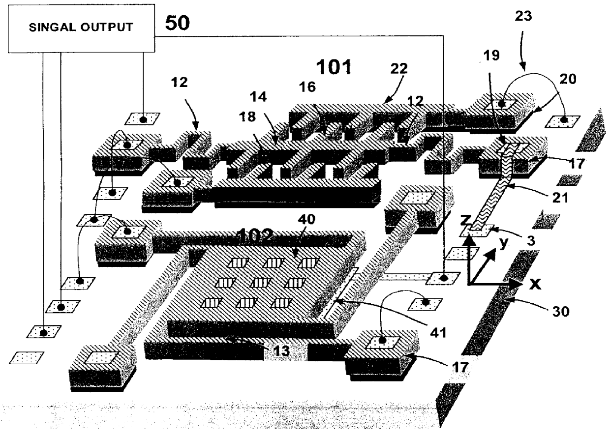
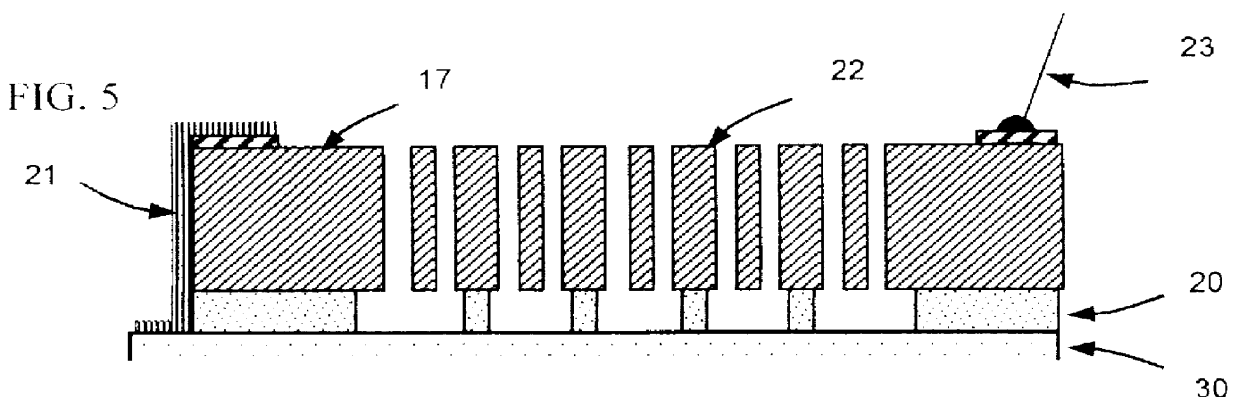
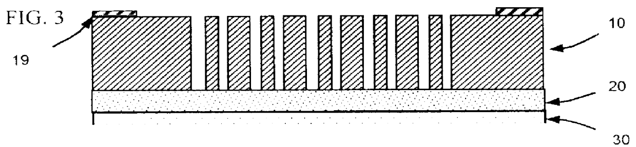
Reference is now made to FIG. 1, wherein the accelerometer embodiment of the present invention is depicted. This accelerometer MEMS device has an x-axis accelerometer 101 and a z-axis accelerometer 102 and a substrate 30. The accelerometers are fabricated from a doped mono-crystalline silicon wafer. The substrate comprises passive or active electrical components such as signal processing circuitry, electrical connections, and capacitive plates. The substrate, if conductive, may also be used as a capacitive plate. The x-axis accelerometer 101 defines (1) a suspended structure comprising central beam 14, a plurality of suspended fingers 16 extending transversely therefrom, two narrow, meandering springs 12, and pads 17, which are bonded to the substrate with a thin layer of organic adhesive 20; (2) a stationary structure comprising two side beams 22, a plurality of stationary fingers 18 extending transversely therefrom that are positioned parallel and adjacent to each said suspended f...


PUM

PropertyMeasurementUnit
thicknessaaaaaaaaaa
pressureaaaaaaaaaa
viscosityaaaaaaaaaa

Abstract

A micro-electro-mechanical device and method of manufacture therefore with a suspended structure formed from mono-crystalline silicon, bonded to a substrate wafer with an organic adhesive layer serving as support and spacer and the rest of the organic adhesive layer serving as a sacrificial layer, which is removed by a dry etch means. Said substrate wafer may contain integrated circuits for sensing and controlling the device.

Description

1. Technical Field of the InventionThe present invention is related to a micro-electro-mechanical device. In particular, the present invention relates to a micro-electro-mechanical device with a suspended structure formed from mono-crystalline silicon, bonded to a substrate wafer with an organic adhesive layer. Still more particularly, the present invention has part of said organic adhesive layer serving as support and spacer and the rest of said organic adhesive layer serving as a sacrificial layer, which is removed by a dry etch means. Even more particularly, the substrate wafer may contain integrated circuits for sensing and controlling said device.2. Description of the Related ArtA micro-electro-mechanical system (MEMS) is a device that transforms mechanical activity into electrical signals and vice versa. A key element in MEMS is a suspended microstructure, which deflects in response to applied force to the microstructure or to a proof mass attached to it. The amount of deflect...

Claims


Application Information

Patent Timeline
Patent Type & Authority Patents(United States)
IPC IPC(8): B81B3/00
CPCB81C1/0019B81C2201/019B81C2201/0108
Inventor WAN, CHANG-FENG
Owner C F WAN
Why Eureka
Try Eureka