Method of manufacturing a thin film transistor involving laser treatment

a technology of laser treatment and thin film, which is applied in the direction of semiconductor devices, electrical devices, transistors, etc., can solve the problems of process which cannot exceed this temperature, lack of heat resistance, and limited substrate type used for display

Inactive Publication Date: 2000-05-16
SEMICON ENERGY LAB CO LTD
View PDF60 Cites 153 Cited by
  • Summary
  • Abstract
  • Description
  • Claims
  • Application Information

AI Technical Summary

Problems solved by technology

However, because the substrate of a liquid crystal display needs to be translucent, the type of substrate to be used with the display is limited.
A glass substrate, a quartz substrate or a plastic substrate may be cited as examples thereof However, a plastic substrate has a problem in that it lacks heat resistance and a quartz substrate has a problem in that it is very expensive.
Because the heat resistance temperature of the glass substrate is normally about 600.degree. C., a process which exceeds this temperature cannot be used for forming the crystal silicon film.
However, the crystal silicon film crystallized from the amorphous silicon film has had a large number of defects caused by dangling bonds and the like.
Because these defects are a factor causing degradation of the characteristics of the TFT, it is necessary to passivate the defects at the interface between the active layer and the gate insulating film and the defects within and at the boundaries of the crystal grains of the silicon of the active layer when fabricating a TFT utilizing such crystal silicon films.
The defects at the grain boundaries in particular are the main factor causing scattering of charge.
However, it is very difficult to passivate the defects at the grain boundary.
In contrast to this, it is difficult to implement a heat treatment at high temperatures when fabricating the TFT on a glass substrate.
Although it is possible to compensate the defect of the grai

Method used


Image

  • Method of manufacturing a thin film transistor involving laser treatment
  • Method of manufacturing a thin film transistor involving laser treatment
  • Method of manufacturing a thin film transistor involving laser treatment

Examples


first embodiment

[First Embodiment]

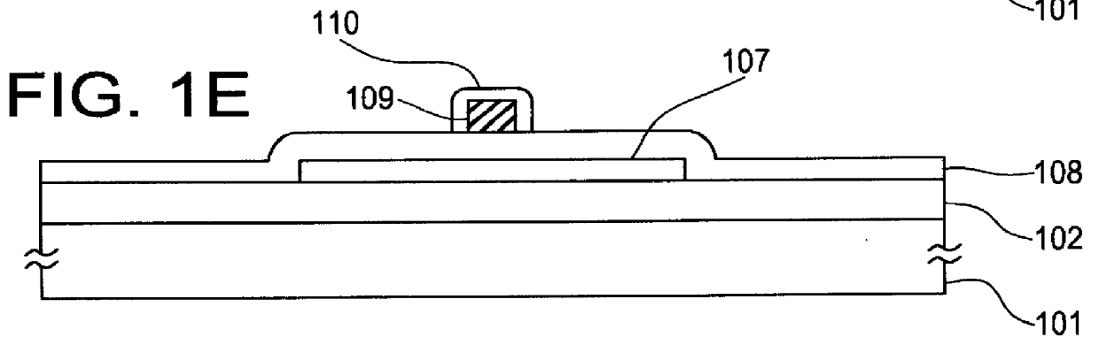
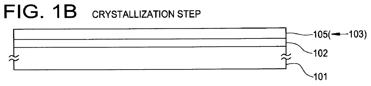
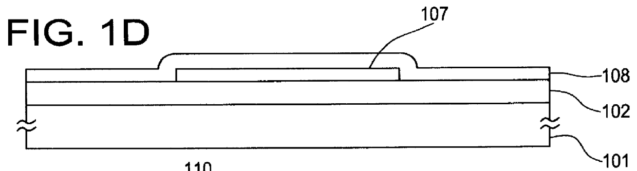
FIGS. 1A-1E and 2A-2B are diagrams for explaining steps for fabricating a TFT according the present embodiment, i.e. section views showing each step. According to the present embodiment, a TFT is fabricated by using a silicon film crystallized by utilizing a catalytic action of a metal element which promotes crystallization of silicon. Nickel is adopted as the metal element in the present embodiment.

As shown in FIG. 1A, a silicon oxide film is formed as an underlying film 102 on a glass substrate 101 (Corning 1737, distortion point: 667.degree. C.) by means of plasma CVD or reduced pressure CVD. Next, a substantially intrinsic (I type) amorphous silicon film 103 is formed by means of plasma CVD or reduced pressure CVD in a thickness of 700 to 1000 angstrom. The thickness of the amorphous silicon film 103 is preferably 700 angstroms.

UV rays are irradiated to the surface of the amorphous silicon film 103 within an oxidizing atmosphere to form an oxide film (not shown...

second embodiment

[Second Embodiment]

FIGS. 3 and 4 are diagrams for explaining steps for fabricating a TFT according to the present embodiment, i.e. section views showing each step. In the present embodiment, a TFT is fabricated using a silicon film crystallized by utilizing a catalytic action of a metal element which promotes crystallization of silicon. Nickel is used as the metal element in the present embodiment.

As shown in FIG. 3A, a silicon oxide film is formed as an underlying film 202 on a glass substrate 201 (Corning 1737, distortion point: 667.degree. .C) in a thickness of 3000 angstrom by means of plasma CVD or reduced pressure CVD. Next, a substantially intrinsic amorphous silicon film 203 is formed by means of plasma CVD or reduced pressure CVD in a thickness of 700 to 1000 angstrom. Here, the thickness of the amorphous silicon film 203 is set at 1000 angstrom.

UV rays are then irradiated to the surface of the amorphous silicon film 203 within an oxidizing atmosphere to form an oxide film ...

third embodiment

[Third Embodiment]

In the present embodiment, a case of fabricating a CMOS type TFT in which a n-channel type TFT and a p-channel type TFT are combined in a complementary manner will be shown. FIG. 5 is a diagram for explaining steps for fabricating the TFT according to the present embodiment. As shown in FIG. 5A, a silicon oxide film is formed as an underlying film 302 on a glass substrate 301 (Corning 1737) in a thickness of 2000 angstrom. Next, a substantially intrinsic amorphous silicon film is formed by the plasma CVD or reduced pressure CVD in a thickness of 700 angstrom. Then, a crystal silicon film 303 is formed by crystallizing the amorphous silicon film by the method shown in the first and second embodiments or by adequate crystallization methods such as heat treatment or irradiation by laser.

A thermal oxide film 304 is formed in a thickness of 200 angstrom as shown in FIG. 5B by implementing thermal oxidation for 2 hours within an oxygen atmosphere containing 400 ppm of NF...


PUM


Abstract

Defects at the grain boundaries of a crystal silicon film, which has been crystallized from an amorphous silicon film, are passivated without using a hydrogen plasma treatment. An underlying film and a crystal silicon film which has been crystallized from an amorphous silicon film are formed on a glass substrate. A thermal oxide film is grown on the surface of the crystal silicon film by heating in an oxygen atmosphere into which NF3 gas has been added. As the thermal oxide film is grown, non-coupled Si is generated. The defects at the grain boundaries of the crystal silicon film are passivated by the additional Si. Then, the thermal oxide film is removed and the crystal silicon film is patterned into an island shape to form an active layer of a TFT. A gate insulating film, a gate electrode and the like are then formed sequentially to complete the TFT.

Description

1. Field of the InventionThe present invention relates to a method for fabricating an insulated gate type semiconductor device such as a thin film transistor.2. Description of Related ArtBecause an active matrix liquid crystal display is small, light and able to display high resolution motion pictures at high speed, it is expected to become one of the most used displays of the future. However, because the substrate of a liquid crystal display needs to be translucent, the type of substrate to be used with the display is limited. A glass substrate, a quartz substrate or a plastic substrate may be cited as examples thereof However, a plastic substrate has a problem in that it lacks heat resistance and a quartz substrate has a problem in that it is very expensive. Its cost is more than 10 times that of a glass substrate especially when it is widened, although it can withstand a high temperature of around 1000.degree. C. Accordingly, the glass substrate is widely used in general for the ...

Claims


Application Information

Patent Timeline
IPC IPC(8): H01L21/28H01L21/02H01L29/66H01L21/70H01L21/20H01L21/336H01L29/786H01L21/322H01L27/12H01L21/84H01L29/49H01L29/40H01L21/77
CPCH01L21/2022H01L21/28158H01L21/3226H01L27/12H01L27/1203H01L27/1277H01L29/66757H01L29/66765H01L29/78621H01L29/78675H01L29/4908H01L21/02488H01L21/02422H01L21/02532H01L21/02675H01L21/02672
Inventor OHTANI, HISASHI
Owner SEMICON ENERGY LAB CO LTD
Why Eureka
Try Eureka