Electron beam projection lithography system (EBPS)

a lithography system and electron beam technology, applied in the field of semiconductor devices and integrated circuits, can solve the problems of high-resolution exposure of resists, lithographic processes often limiting the throughput of production lines, and relatively time-consuming

Inactive Publication Date: 2000-05-30
IBM CORP
View PDF6 Cites 52 Cited by
  • Summary
  • Abstract
  • Description
  • Claims
  • Application Information

AI Technical Summary

Benefits of technology

It is another object of the invention to provide ranges of physical configuration and operating parameters for fundamental elements of an electron beam lithographic exposure system, in combination, which will reliably provide high resolution and high throughput in feature size significantly smaller than quarter-micron regimes.

Problems solved by technology

A lithographic process, itself requires multiple steps of at least applying a resist, drying the resist, exposing the resist, developing the resist and then performing a material deposition or removal process, all of which are relatively time-consuming.
Therefore, the lithographic processes are often a limiting factor in production line throughput.
Additionally, the small feature sizes of modern and foreseeable integrated circuits require extremely high-resolution exposures of the resist to be made.
Optical technology has advanced to the point that resolution is essentially limited by diffraction (or, more generally, interference effects of the radiation) but not significantly by imperfections of the optics known as aberrations.
However, to delineate a desired pattern over a chip of transverse dimensions in the range of several millimeters, the exposure is essentially a sequential process carried out over many thousands or millions of spots or "pixels" (although, as a practical matter, a spot can contain more than one pixel, for example, about 100 pixels in a shaped beam system; the term "pixel" being more generally equated with system resolution) and is therefore much more time-consuming than an exposure in an optical system in which an entire chip pattern can be exposed in a single flash.
However, some practical limitations of projection systems are encountered at even relatively small reticle sizes and relatively low throughputs.
Further, the electron emitting surface of the cathode electron source is imaged at the reticle and the physical size of the cathode required to produce sufficiently uniform illumination across the entire reticle is not available at the present time.
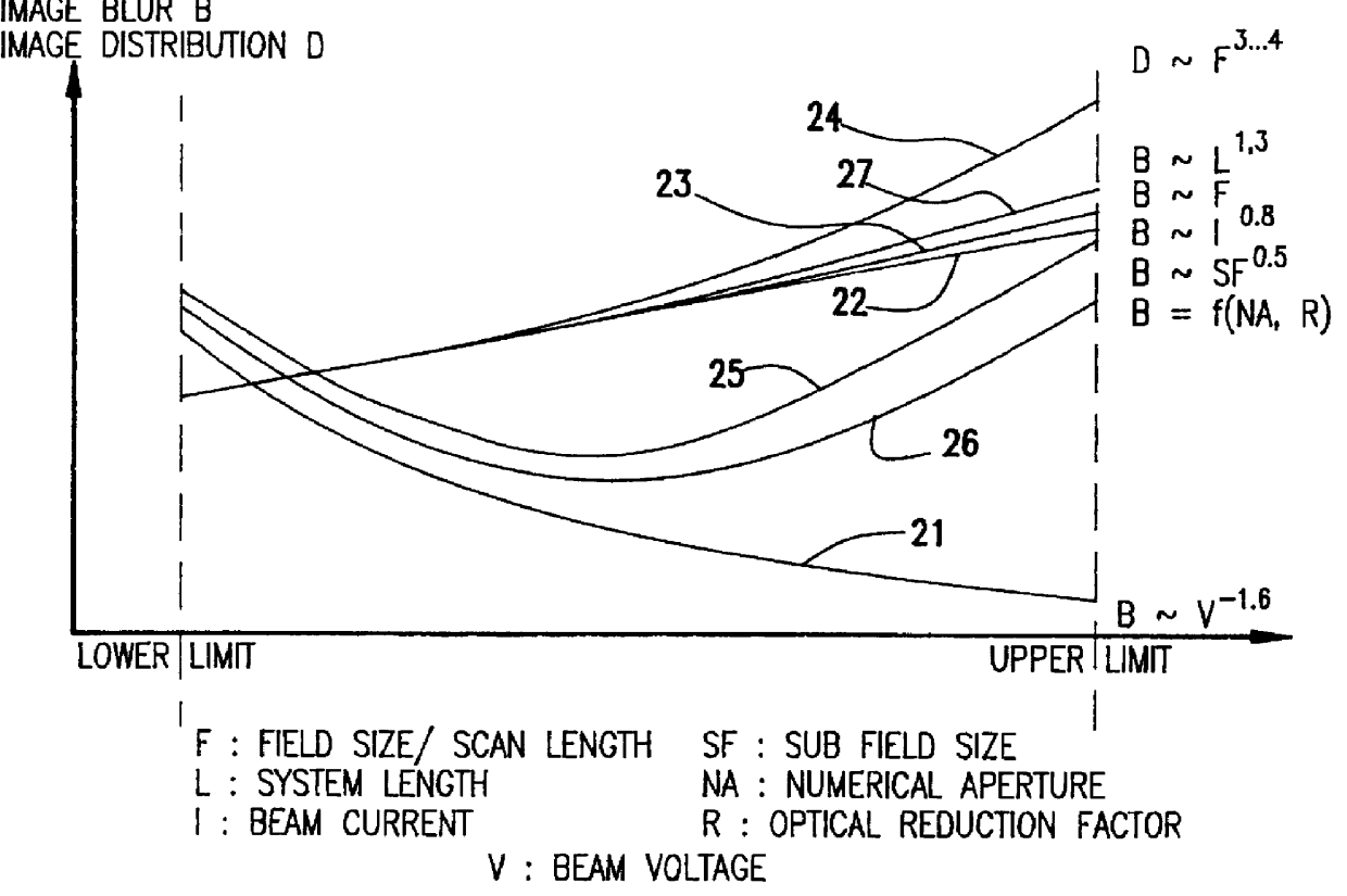
However, while specific forms of these fundamental elements described in the U.S. Patents and Patent Applications incorporated by reference above are directed to improvement of resolution, reliability or speed of operation, it has not been demonstrated that these elements will fully cooperate to unconditionally provide high resolution and, simultaneously, high throughput, adequate for current and foreseeable integrated circuit designs and ground rules.
On the contrary, unpredictable criticalities have been found to arise at smaller feature size ground rule regimes.
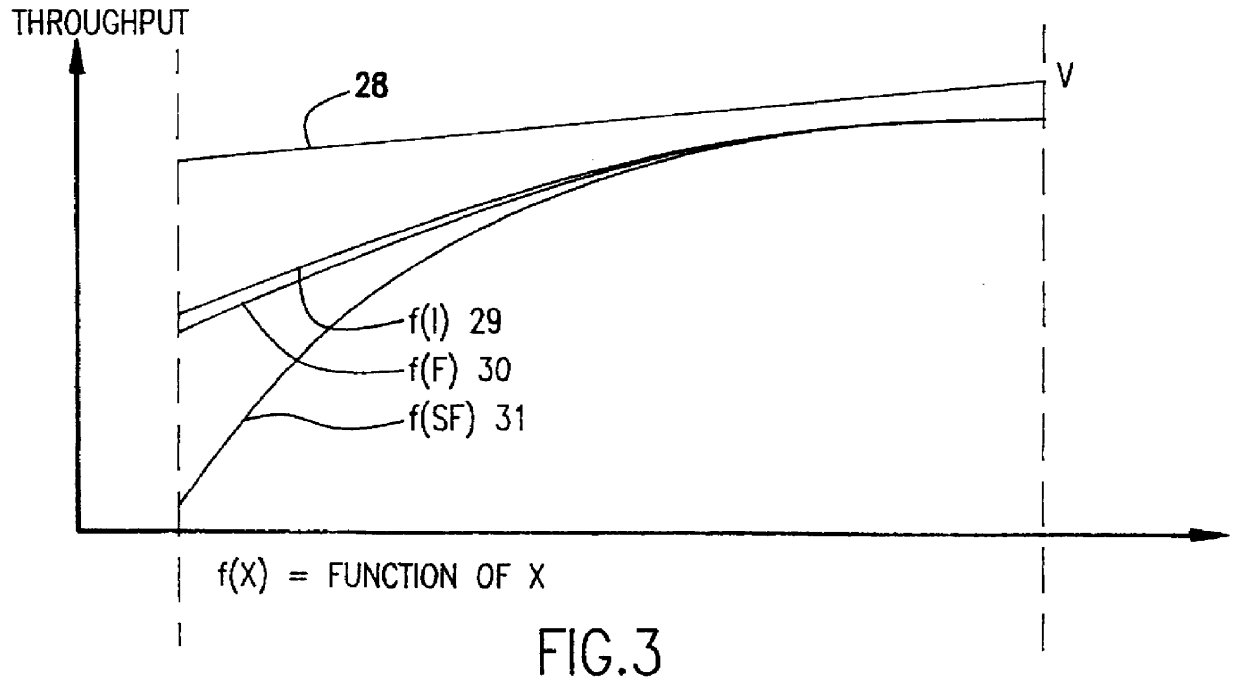
However, increasing the acceleration voltage effectively reduces resist sensitivity, for which increased beam current might be used to compensate to maintain throughput.
Increased beam current increases Coulomb interactions between electrons and resultant aberrations, yielding only relatively slight gains while increasing the power dissipation requirements at beam-limiting diaphragms or apertures and of beam positioning and deflection devices, ultimately affecting beam stability and placement accuracy.
Heating of the wafer or portions thereof causes uncontrollable changes in the resist chemistry and / or expansion and distortion of the wafer which may result in so-called overlay errors in the exposure pattern in quantitative dependence on beam placement, resist sensitivity and the like.
However, increase of the e-beam column length increases geometric aberrations as well as those due to Coulomb interactions.
Compensation by scaling of the electron beam energy or accelerating voltage compromises throughput unless the beam current is further increased which may, in turn, compromise resolution and overlay accuracy, as discussed above.
Again, the quantitative change in aberrations is also affected by magnification, lens configuration and the like in addition to the trade-off between field size and lens and corrector accuracy and the accuracy of positioning systems (which exhibit a limitation given by the speed-accuracy product of their design) for the reticle and wafer.
Thus, it can be appreciated that the physical configuration and operating parameters needed to apply the preferred, known, technologies discussed in the above-incorporated U.S. Patents and Patent Applications, in combination, to lithographic processes in smaller than quarter micron regimes is not at all straightforward, much less leading toward optimization, and the level of skill in the art does not assure success of any particular combination of structures of fundamental system elements at smaller feature size regimes consistent with maintaining an acceptable throughput of the system, much less a throughput comparable to optical exposure systems.
Adjustment of dwell time and the use of repeated scans is utilized in Berger to keep overlay error within acceptable limits but, understandably, may compromise throughput.
While Berger may be effective to produce acceptable results with acceptable throughput in half-micron feature size regimes, it does not provide a methodology to derive high throughput consistent with high resolution which is necessarily effective in the much smaller feature size regimes now required.

Method used


Image

  • Electron beam projection lithography system (EBPS)
  • Electron beam projection lithography system (EBPS)
  • Electron beam projection lithography system (EBPS)

Examples


Embodiment Construction

Referring now to the drawings, and more particularly to FIG. 1, there is schematically shown, in cross-section, an electron beam projection system to which the invention is applicable. This e-beam projection system is similar to that described in the above-incorporated U.S. Pat. No. 5,545,902 to which the present invention may be applied. The form of illustration is highly schematic and simplified in the interest of readily conveying an understanding of the invention. The invention is, however, applicable to other e-beam projection systems, such as that disclosed in the above-incorporated U.S. Pat. No. 5,635,719, and including fundamental elements advantageously incorporating particular forms thereof described in the above-incorporated U.S. Patents and Patent Applications as will be understood by those skilled in the art in light of the following description of the invention. It is also to be understood that while the basic combination of fundamental elements depicted in FIG. 1 is k...


PUM

PropertyMeasurementUnit
diameteraaaaaaaaaa
sizeaaaaaaaaaa
lengthaaaaaaaaaa

Abstract

Numerous largely unpredictable criticalities of operating parameters arise in electron beam projection lithography systems to maintain throughput comparable to optical projection lithography systems as minimum feature size is reduced below one-half micron and resolution requirements are increased. Using an electron beam projection lithography system having a high emittance electron source, variable axis lenses, curvilinear beam trajectory and constant reticle and / or target motion in a dual scanning mode wherein the target and / or wafer is constantly moved orthogonally to the direction of beam scan, high throughput is obtained consistent with 0.1 mu m feature size ground rules utilizing a column length of greater than 400 mm, a beam current of between about 4 and 35 mu A, a beam energy of between about 75 and 175 kV, a sub-field size between about 0.1 and 0.5 mm at the target at an optical reduction factor between about 3:1 and 5:1, a numerical aperture greater than 2 mrad and preferably between about 3 and 8 mrad and a scan length between about 20 mm and 55 mm. Reticle and target speed preferably differ by about the optical reduction factor.

Description

1. Field of the InventionThe present invention generally relates to the manufacture of semiconductor devices and integrated circuits and, more particularly, to lithographic processes and tools for making lithographic resist exposure with an electron beam.2. Description of the Prior ArtLithographic processes are generally required in the manufacture of semiconductor integrated circuits. Even though there is a trend in the manufacture of integrated circuits to employ processes and element designs in which many processes are carried out in a self-aligned manner (both to avoid some lithographic processes and to produce structures at smaller size than can be accomplished lithographically), at least one lithographic process to define element locations is invariably required. A lithographic process, itself requires multiple steps of at least applying a resist, drying the resist, exposing the resist, developing the resist and then performing a material deposition or removal process, all of ...

Claims


Application Information

Patent Timeline
Patent Type & Authority Patents(United States)
IPC IPC(8): G03F7/20H01J37/317H01J37/305H01L21/027
CPCB82Y10/00B82Y40/00H01J37/3174G03F7/2059H01J2237/31766
Inventor GOLLADAY, STEVEN D.PETRIC, PAUL F.PFEIFFER, HANS C.STICKEL, WERNER
Owner IBM CORP
Why Eureka
Try Eureka