Hard graphite-like material bonded by diamond-like framework
a graphite-like material and diamond-like structure technology, applied in the field of hard carbon materials, can solve the problems of reducing the productivity of composite materials, increasing the cost correspondingly, and limiting the approach by structural resolution
- Summary
- Abstract
- Description
- Claims
- Application Information
AI Technical Summary
Benefits of technology
Problems solved by technology
Method used
Image
Examples
example 2
The material of the invention was deposited under the following process conditions:
The material of Example 2 exhibits high strength and elastic modules. Areas of applications of material fabricated in accordance with Example 2 include hard protective coatings, in particular, protective coating for steel tools.
example 3
The material was deposited under similar conditions to Example 1, except the energy of the particles was lower, while the substrate temperature higher. Also, the distance between the plasmatron and substrate was less, and the growth rate was correspondingly higher in contrast to Example 1. The material was deposited under the following process conditions:
This material can be used for protective coating for cutting tools, in particular, protective coating for high-speed steel cutting tools. Mills with different diameters and shape manufactured in different countries (U.S.A., Japan, Israel) were coated with material from Example 3 and tested under standard conditions of steel cutting. The tests (data not shown) showed a 62 to 65% increase of mill life when coated with the material of the invention.
example 4
The material was deposited under similar conditions to Example 1, except that: the particle energy was 50 eV, the substrate temperature was 530.degree. C., the distance between the plasmatron and substrate was 4 cm, the growth rate was 20 .mu.m hours and the process time was 15 hours. The material was deposited under the following process conditions:
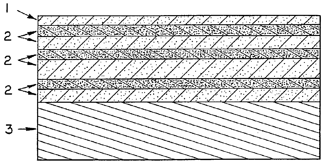
The silicon substrate was scratched from back to side using a diamond tip. The 2.times.2 cm.sup.2 pieces were then fabricated. Thereafter, the substrates were etched out from the pieces and free-standing material was bonded with a high-temperature compound having a composition similar to the deposited materials composition. 2.times.2.times.2 cm.sup.3 bulk material was obtained having a total thickness of 63 compound interlayers (about 800 em). This material can be used for protective coatings, as well as heat-conductive insulated substrates for electronic devices. The material can also be used as a basic constructive material for micro-m...
PUM
| Property | Measurement | Unit |
|---|---|---|
| Linear density | aaaaa | aaaaa |
| Thickness | aaaaa | aaaaa |
| Thickness | aaaaa | aaaaa |
Abstract
Description
Claims
Application Information


