Method for determining the temperature of semiconductor substrates from bandgap spectra

a technology of semiconductor substrates and bandgap spectra, which is applied in the direction of instruments, heat measurement, measurement devices, etc., can solve the problems of insufficient accuracy, inability to physically contact the wafer with a temperature sensor, and inability to achieve accurate measurement results

a technology of semiconductor substrates and bandgap spectra, which is applied in the direction of instruments, heat measurement, measurement devices, etc., can solve the problems of insufficient accuracy, inability to physically contact the wafer with a temperature sensor, and inability to achieve accurate measurement results

US6116779AInactive Publication Date: 2000-09-12JOHNSON SHANE R +1

Image

  • Method for determining the temperature of semiconductor substrates from bandgap spectra
  • Method for determining the temperature of semiconductor substrates from bandgap spectra
  • Method for determining the temperature of semiconductor substrates from bandgap spectra

Examples


Embodiment Construction

Introduction and Description of the Problem

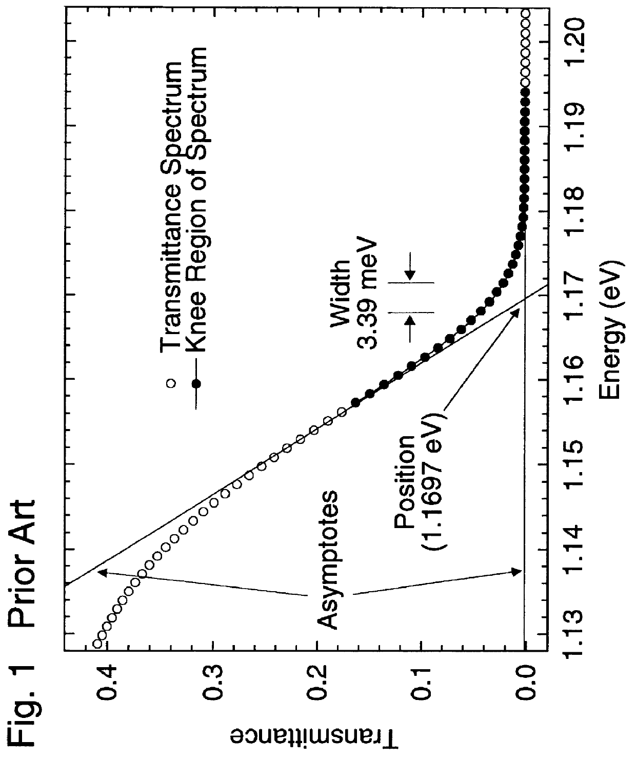
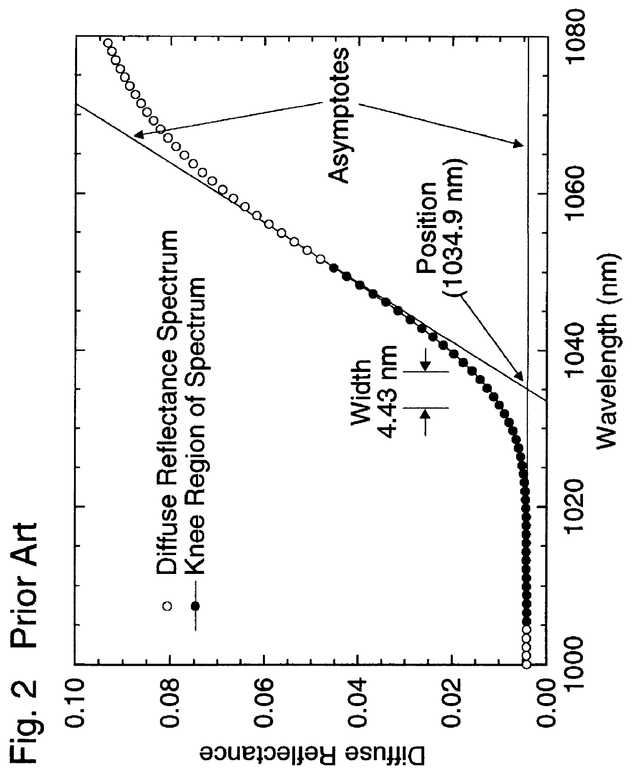
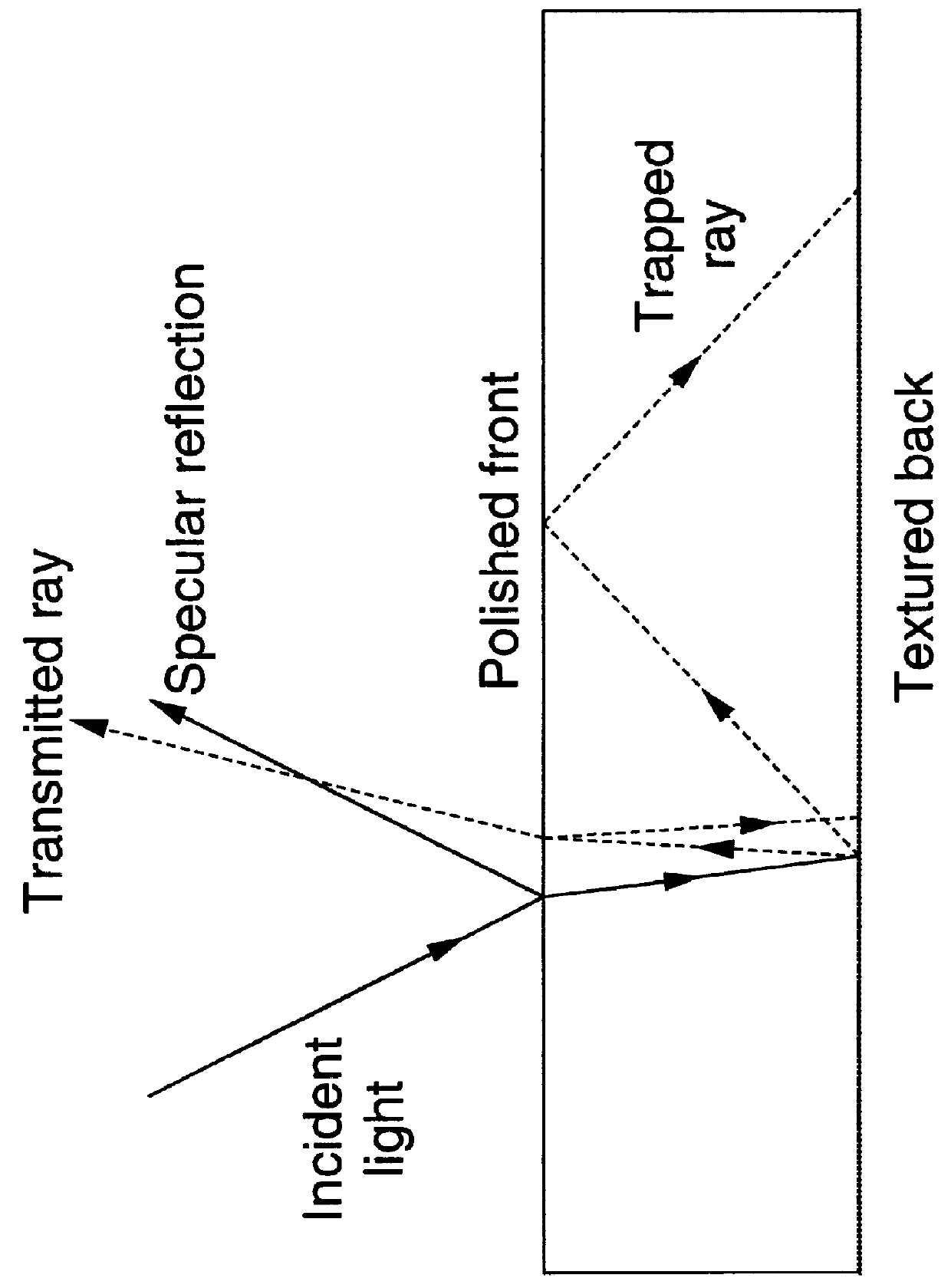
As critical dimensions in semiconductor devices have become progressively smaller and device designs progressively more sophisticated, the requirements for control over the fabrication processes have become more stringent. For example semiconductor lasers for telecommunications will in the near future contain quantum well or multiple quantum well structures in which the allowed tolerances on the individual layer thicknesses will be in the range of a few atomic layers. At the same time the composition of these layers will need to be controlled to of order 0.3% or better to obtain adequate lattice constant match to the substrate and desirable emission wavelengths. Ideally the optimum properties of the layers need to be held fixed over the entire surface of a 3 inch diameter wafer in order to achieve a high yield of good devices.

Semiconductor lasers are now manufactured from compound semiconductor alloys containing two to four different alloyi...


PUM

PropertyMeasurementUnit
temperatureaaaaaaaaaa
diameteraaaaaaaaaa

Abstract

An optical method for measuring the temperature of a substrate material with a temperature dependent band edge. In this method both the position and the width of the knee of the band edge spectrum of the substrate are used to determine temperature. The width of the knee is used to correct for the spurious shifts in the position of the knee caused by: (i) thin film interference in a deposited layer on the substrate; (ii) anisotropic scattering at the back of the substrate; (iii) the spectral variation in the absorptance of deposited layers that absorb in the vicinity of the band edge of the substrate; and (iv) the spectral dependence in the optical response of the wavelength selective detection system used to obtain the band edge spectrum of the substrate. The adjusted position of the knee is used to calculate the substrate temperature from a predetermined calibration curve. This algorithm is suitable for real-time applications as the information needed to correct the knee position is obtained from the spectrum itself. Using a model for the temperature dependent shape of the absorption edge in GaAs and InP, the effect of substrate thickness and the optical geometry of the method used to determine the band edge spectrum, are incorporated into the calibration curve.

Description

This invention relates to thermometry and to methods and devices for making non-contact measurements of the temperature of semiconductor substrate materials in various process environments including molecular beam epitaxy, chemical vapor deposition, plasma assisted chemical vapor deposition, plasma etching, metal organic chemical vapor deposition, sputtering, and rapid thermal annealing.The substrate temperature is an important parameter in thin film deposition and semiconductor processing operations. The substrate temperature and its uniformity can have a large effect on the quality and composition of the deposited layers. In molecular beam epitaxy for example, the substrate wafer is normally heated radiatively and rotated during the thin film growth operation. Physical contact between the wafer and a temperature sensor is not practical nor desirable because the sensor itself would cause local perturbations in temperature or even contamination of the substrate. Even if the wafer is...

Claims


Application Information

Patent Timeline
12 Sep 2000
Publication
US6116779A
IPC
G01K11/00; G01K11/14
CPC
G01K11/14
Inventors
JOHNSON, SHANE R.; TIEDJE, J. THOMAS