Versatile gate-array cell with interstitial transistors for compact flip-flops with set or clear

a gate array and transistor technology, applied in logic circuits using specific components, pulse generators, pulse techniques, etc., can solve the problems of complex interconnection or wiring of transistors in gate array cells, less compact arrays of transistors than custom circuits, and increased production costs of gate array circuit implementations. achieve the effect of facilitating the elimination of transmission gates, reducing area, and improving clock-to-output delay

Inactive Publication Date: 2000-11-07
DIODES INC
View PDF3 Cites 21 Cited by
  • Summary
  • Abstract
  • Description
  • Claims
  • Application Information

AI Technical Summary

Benefits of technology

The NAND gates for the set or clear functions are replaced by simple pull-up or pull-down transistors and clock control. The pull-down transistor pulls low the input of a cross-coupled inverter latch, writing a low to the master latch. The cleared master then writes the zero to the slave latch through an open pass transistor. The output is buffered by an inverter. Thus output loading does not affect the slave latch.The flip-flop with clear of FIG. 4 requires only 21 transistors compared to 28 transistors for the prior-art of FIG. 1. This is a reduction of 25% of the number of transistors. Area is further reduced by using smaller-size transistors for the feedback inverters of the master and slave latches. Interconnection wiring is simplified second-layer metal is not needed. Wiring from p-channel transistors to n-channel transistors for transmission gates is not needed with the simple pass transistors. The clock-to-output delay is improved since slower NAND gates are replaced by inverters.A wide variety of latches, flip-flops, and logic gates can be implemented with the gate-array cell with smaller and larger transistors. The cell is efficient since the smaller transistors are used for feedback inverters, where a large current drive is not necessary; indeed is undesirable. Using the smaller feedback transistors facilitates the elimination of the transmission gate in the feedback path, further reducing flip-flop area.Providing the pair of smaller transistors in each gate-array cell may seem wasteful, but the small size of these transistors allows them to fit between the larger transistors' polysilicon contact tabs. The smaller transistors are formed in the interstitial area between the larger transistors so that the area of the cell is expanded only slightly, and only in height and not in width. Thus the additional area for the smaller transistors is minimal. In return, the smaller transistors increase the number of transistors in each cell by 50%, allowing more circuitry to be squeezed into fewer cells. The dramatic reductions in the number of gate-array cells required for the basic functions shown in Table 1 testifies to the usefulness of the cell with larger and smaller transistors.The smaller transistors enable a reduction in the number of transistors required. The smaller transistors allow a feedback inverter to directly connect to the input, since the input can easily over-power the feedback current. This is not possible when only larger transistors are used. Transmission gates are eliminated when direct feedback is feasible. Thus, the smaller transistors enable a reduction in transistor count as well as being smaller in size.

Problems solved by technology

While such gate-array chips are effective at reducing costs, often the transistors are arrayed less compactly than custom circuits.
The larger area required increases production costs for a gate-array implementation of a circuit compared to a custom implementation of the circuit.
Interconnection or wiring of the transistors in a gate-array cell is complicated by the full transmission gates, since the p-channel and n-channel transistors are formed in remote portions of each gate-array cell.
Thus space is wasted.
Many modern circuits are so complex that fully synchronous design methods are used anyway.
However, Hashimoto's cell is inefficient since the smaller-size gate is always connected to a larger-size gate in a single polysilicon line.
Thus larger and smaller gates are always formed together, and the smaller gate suffers additional delay from the loading of the larger gate even when the larger gate is not used.
While this arrangement is useful for memory cells needing smaller pass transistors, it has limited application for logic gates.
The cell placement is inefficient because of the non-homogeneous cell structure.
The smaller transistors cannot be used for many logic circuits.
Eliminating the feedback transmission gates in the prior-art master or slave stage could cause a failure because the master's or slave's feedback inverters have about the same current drive as the current driven into the slave stage from the D-input or master stage.

Method used


Image

  • Versatile gate-array cell with interstitial transistors for compact flip-flops with set or clear
  • Versatile gate-array cell with interstitial transistors for compact flip-flops with set or clear
  • Versatile gate-array cell with interstitial transistors for compact flip-flops with set or clear

Examples


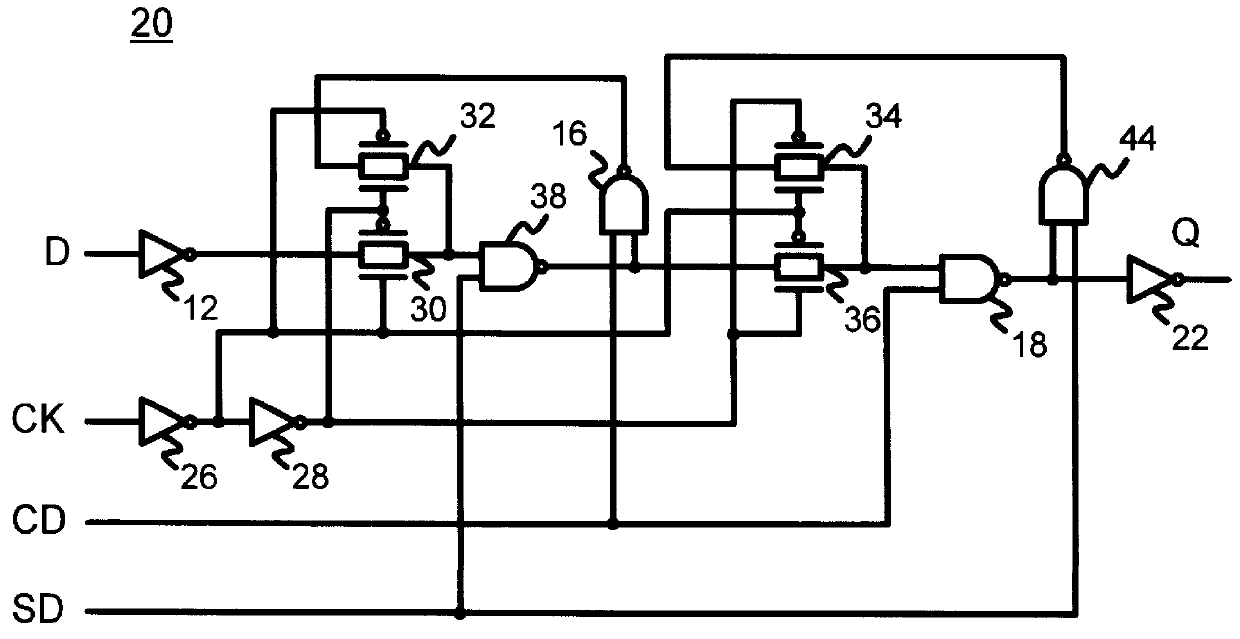
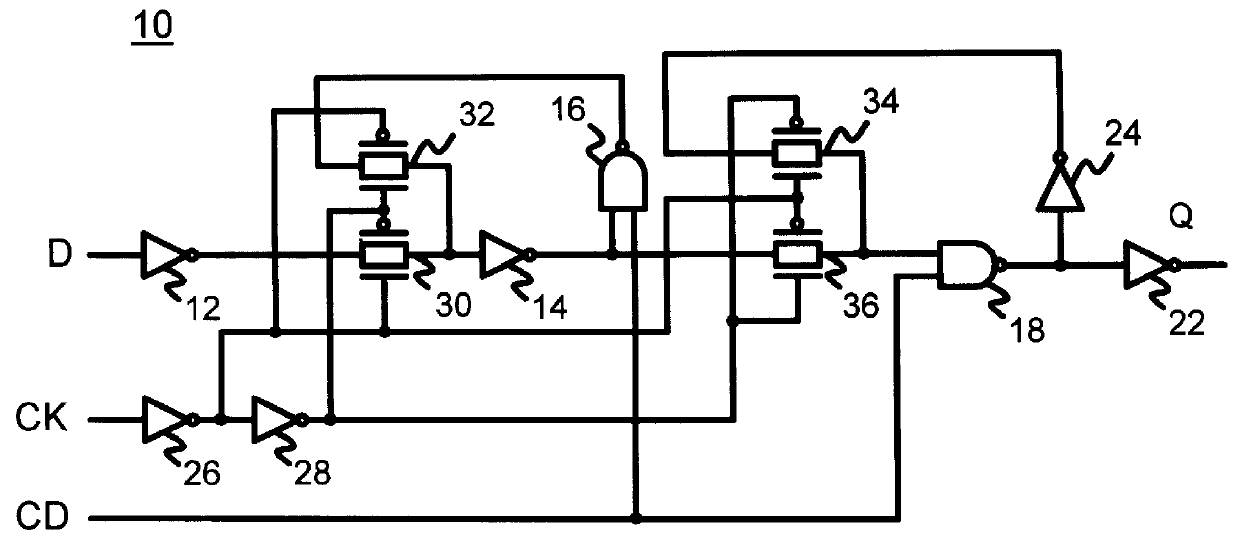
Embodiment Construction

Several other embodiments are contemplated by the inventor. For example the smaller-size gates could have their transconductance reduced even further than possible by reducing the gate width W by increasing the gate length L above the minimum used for other gates. The gate-array cell can be arrayed in a chip with custom macro-blocks such as memory arrays or processor blocks. The gate-array cell may also be used in a smaller gate-array region of a larger custom chip, or as standard cells. The gate-array cell may be mirrored or flipped as needed rather than strictly arrayed without mirroring.

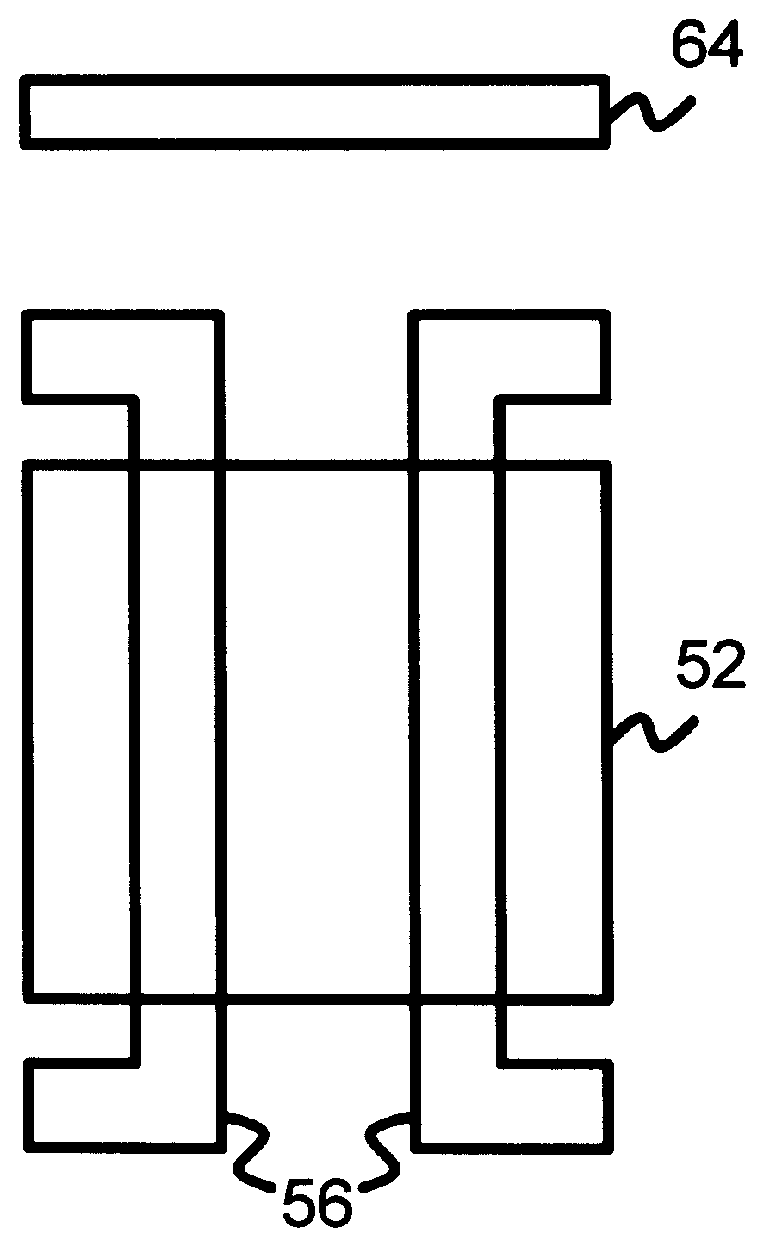
The cell layout can be modified or optimized somewhat, such as by rounding or cropping corners of active areas, polysilicon lines, and metal lines. The poysilicon gates can be merged or separate. The cell with larger and smaller transistors can be fit into an existing form factor of standard gate-array cells with only large transistors by shrinking the large transistors somewhat to make room for t...


PUM


Abstract

A gate-array cell uses smaller and larger transistors. Four larger transistors are provided: two n-channel and two p-channel. A small p-channel transistor is placed between the contact tabs of the polysilicon lines of the two larger p-channel transistors, and between the p-channel transistors and a N-well tap. A small n-channel transistor is similarly placed between the contact tabs of polysilicon lines of the two larger n-channel transistors, and between the n-channel transistors and a P-well tap. The cell is slightly expanded in height to accommodate the two smaller transistors. The smaller transistors enable a reduction in the number of transistors required for latches and flip-flops. The smaller transistors allow a feedback inverter to directly connect to an input, since the input can easily over-power the feedback current. This is not possible for standard gate array cells having only one transistor size. Transmission gates are eliminated when direct feedback is feasible. Thus, the smaller transistors enable a reduction in transistor count as well as being smaller in size. Clear and set are provided by larger pull-down or pull-up transistors rather than NAND gates, since the larger pull-down and pull-up transistors can easily over-power the feedback inverters.

Description

1. Field of the InventionThis invention relates to semiconductor logic arrays, and more particularly to gate-array cell layouts for flip-flops with set and clear.2. Description of the Related ArtHigher densities of integration of semiconductor circuits have yielded a dramatic reduction in electronic component cost. Semi-custom chips reduce the initial tooling costs for new circuits (the non-recurring engineering or NRE costs). Semi-custom chips reduce tooling costs by customizing relatively few masking layers while using standard layouts for other masking layers. For example, gate-array semi-custom chips have an array of transistors formed in a standard layout in the base masking layers, such as the active-area, implant, polysilicon layers. Upper masking layers, such as contacts, metals, and vias are customized for each customer's circuit design.While such gate-array chips are effective at reducing costs, often the transistors are arrayed less compactly than custom circuits. The lar...

Claims


Application Information

Patent Timeline
Patent Type & Authority Patents(United States)
IPC IPC(8): H01L27/118
CPCH01L27/11807
Inventor WONG, ANTHONY YAP
Owner DIODES INC
Why Eureka
Try Eureka