Matrix-inductor soldering apparatus and device

Inactive Publication Date: 2001-02-13
TRUCCO HORACIO ANDRES
View PDF6 Cites 29 Cited by
  • Summary
  • Abstract
  • Description
  • Claims
  • Application Information

AI Technical Summary

Benefits of technology

The general objective of my invention is to provide the electronic manufacturing or electronic packaging industry with a new, safe, reliable, speedier and useful device for soldering components to a PCB. Because my invention only heats the leads and pads to be joined by solder while the rest of a component (namely its casing or housing) remains relatively cold, utilization of my invention will help to reduce manufactured-product cost. Components rated to tolerate much lower temperature exposure (than now required when utilizing reflow or wave solder processes) will be acceptable. Also my invention allows to improve the quality and re

Problems solved by technology

Both processes exhibit inherit disadvantages that indeed, increase the cost of the final product, generate rejects, require rework and reduce the reliability of the final product.
The electronic manufacturing industry accepts these inherit drawbacks and shortcomings, and works around them, for lack of a more suitable soldering process.
Therefore, all electronic components must be unnecessarily temperature-overrated to tolerate or survive the soldering process.
This requirement for high-temperature-exposure survival increases the cost of every component to be soldered to a PCB.
During the soldering process, thermal shock (due to a fast heating rate) can crack certain components, in particular ceramic capacitors, increasing rejects and/or requiring costly rework.
Fast heating of plastic IC pa

Method used


Image

  • Matrix-inductor soldering apparatus and device
  • Matrix-inductor soldering apparatus and device
  • Matrix-inductor soldering apparatus and device

Examples


Embodiment Construction

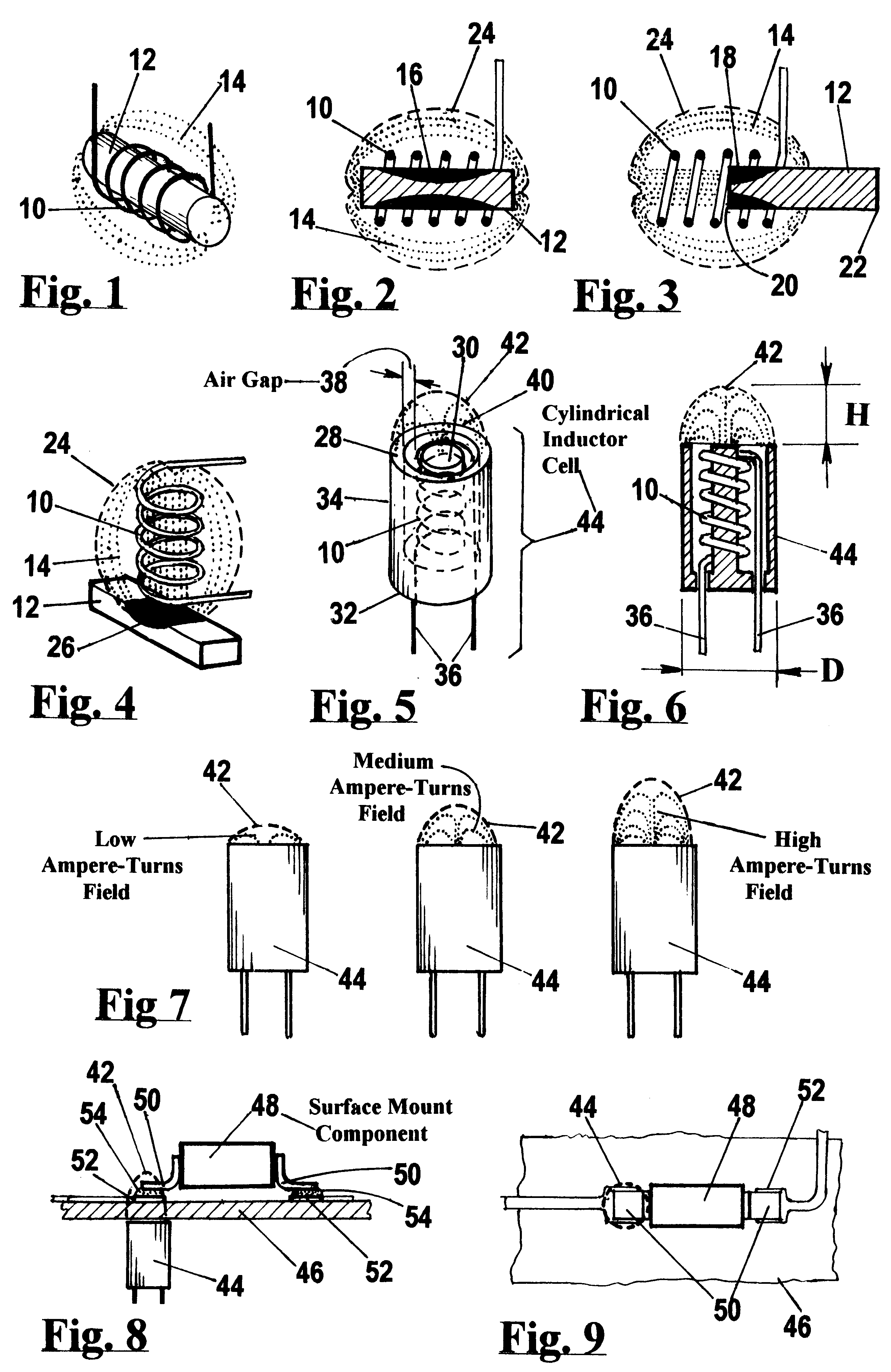
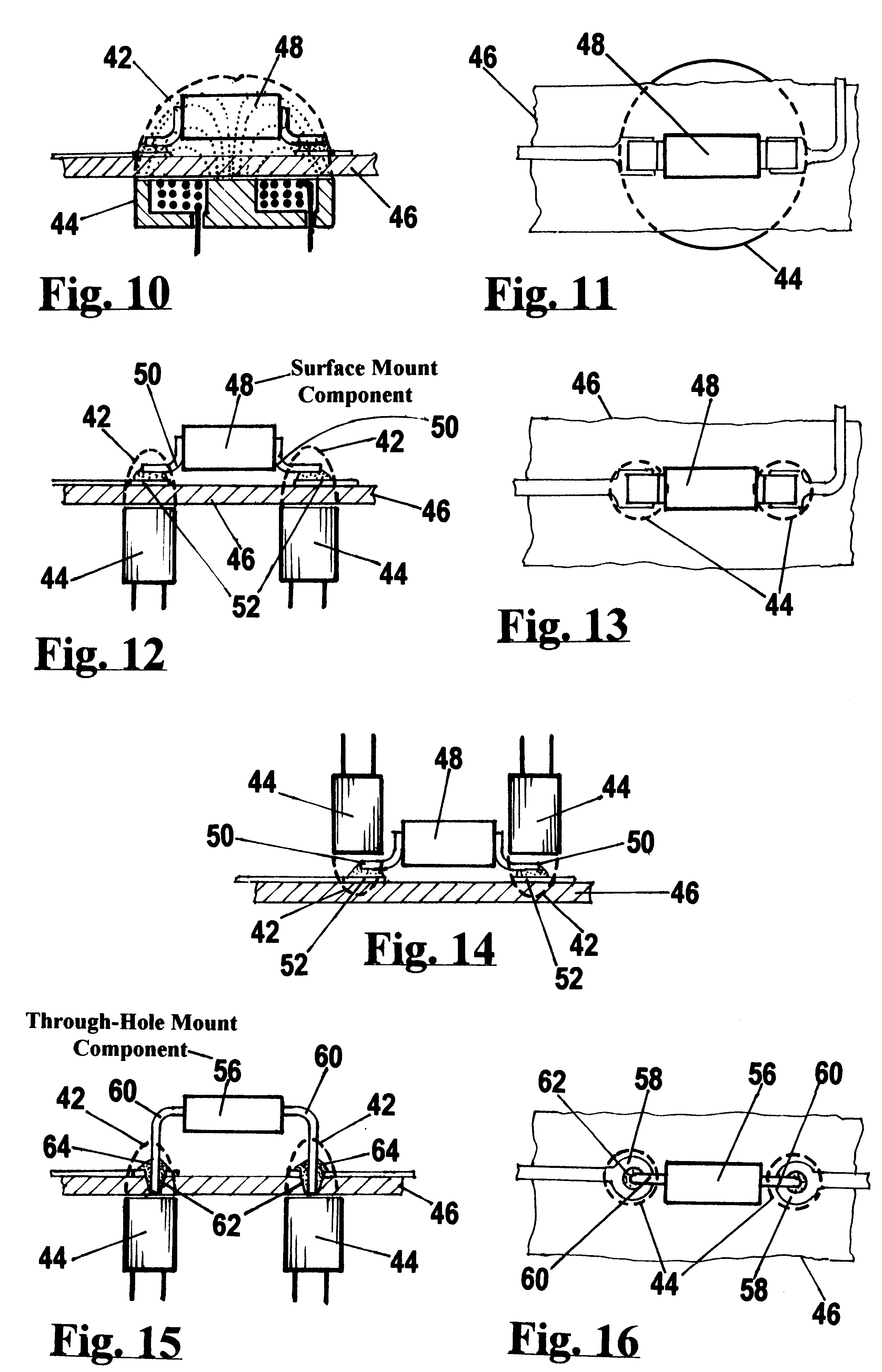
Now, aided by FIGS. 17 through 31, I shall illustrate and describe the novel and non-obvious components that form part of the embodiments of my invention. Because the actual embodiments of my invention also include items-of-commerce recognized as public-domain prior-art, the preferred embodiments will be illustrated afterwards in FIGS. 32 through 37 and described in the next part of this specification.

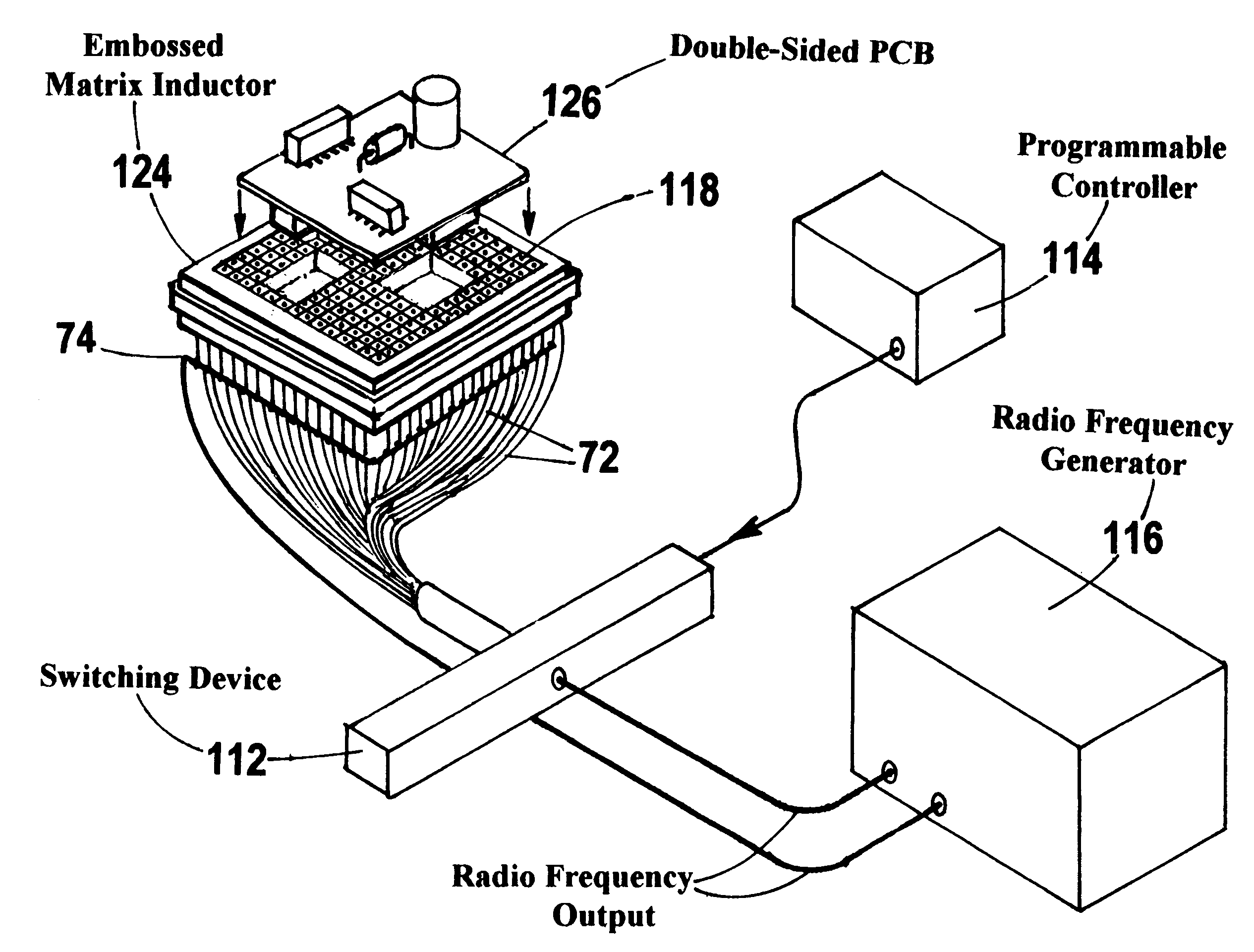
FIG. 17 shows, in perspective view, a multiplicity of cylindrical inductor cells 44 placed side-by-side conforming to a matrix arrangement and held together by an encircling or holding frame 66. Cells' 44 individual air gaps 38 are all facing in the same direction, upwards, and are all contained on a flat upper surface, or top face 68. From every inductor cell 44, a pair of terminals 36-36 emerges beneath the underside or base face 70. One terminal 36 from each and every inductor cell 44 is outfitted with an extension wire 72. The other remaining terminals 36 are all interconnected tog...


PUM

PropertyMeasurementUnit
Temperatureaaaaaaaaaa
Thicknessaaaaaaaaaa
Dielectric polarization enthalpyaaaaaaaaaa

Abstract

A new apparatus and process for soldering surface-mount and through-hole type electronic components into a printed circuit board (PCB) in an automated fashion utilizing localized electromagnetic induction heating. Current manufacture technology for packaging electronic components depends exclusively on the reflow and wave soldering processes. Both processes heat up to relatively high temperature the entire assembly, namely its PCB and all the electronic components been soldered into it. Such high temperature environment frequently causes components damage resulting in rejects and/or demanding rework. With this invention however, during a soldering operation only the leads and pads, or joints, being soldered are heated but neither the body, or casing, of said electronic components nor the dielectric material forming said PCB are heated. Because of this selectively localized heating, the invention permits to reduce cost and improve the quality and reliability of manufactured products. This invention consumes about 200 times less energy than the reflow and wave soldering processes. Also allows in-process, and in-situ, testing of soldered joints quality thus permitting rework before final assembly of a PCB is completed. This invention also provides for an useful de-soldering apparatus.

Description

This invention relates to a novel soldering apparatus and soldering process for joining electronic components to a printed circuit board utilizing localized electromagnetic induction heating.BACKGROUND-DESCRIPTION OF THE PRIOR ARTThe manufacture of most modern electronic products require a printed circuit board (PCB) that allows to electrically interconnect a variety of electronic components and also holds them together in a relatively rigid condition. Many types of components are placed over a single PCB. Electronic components such as resistors, capacitors, inductors, transformers, integrated circuit (IC) packages, connectors, headers, RF shields, LEDs, switches, board interface systems, battery sockets, etc. are electrically connected and restrained by means of soldered joints. These joints can be obtained by three methods: hand soldering, the wave soldering process and by the reflow soldering process.Mass production exclusively utilizes wave and reflow soldering processes, either...

Claims


Application Information

Patent Timeline
IPC IPC(8): B23K1/002H05K3/34H05B6/02H05B6/06H05B6/10H05B6/40
CPCB23K1/002H05B6/40H05K3/3494B23K2201/40Y10T29/49211H05K3/3415H05K2203/101H05B2213/03B23K2101/40
Inventor TRUCCO, HORACIO ANDRES
Owner TRUCCO HORACIO ANDRES
Why Eureka
Try Eureka