Eureka AIR delivers breakthrough ideas for toughest innovation challenges, trusted by R&D personnel around the world.

Semiconductor device and method for manufacturing the same

Inactive Publication Date: 2001-04-03
SEMICON ENERGY LAB CO LTD
View PDF79 Cites 50 Cited by
  • Summary
  • Abstract
  • Description
  • Claims
  • Application Information

AI Technical Summary

Benefits of technology

Furthermore, the inventors have discovered that a concentration of electron traps is undesirably high when the silicon oxide film is formed by an organic silane through CVD and the inventor considered that the traps are related to Si--OH bondings. In accordance with another aspect of the invention, the silicon oxide formed from an organic silane is annealed with a nitrogen containing atmosphere, for example, NH.sub.3, N.sub.2 H.sub.4, N.sub.2 and N.sub.2 O at a temperature from 400-850.degree. C., thereby, breaking the Si--OH bondings and improving the reliability of the gate insulated structure.
In case irradiation is effected for a short period of time using UV as the light source, a laser operated in pulses, such as the excimer laser, is most preferred. An excimer laser has a pulse width of 100 nsec or less.
The thermal oxide film which is obtained by either irradiating an intense light or by annealing at a medium temperature is generally provided at a thickness of from 20 to 200 .ANG., and representatively, at a thickness of 100 .ANG.. It differs from a known film obtained by PVD or CVD, and is an extremely dense film of a uniform thickness free from pinholes. Furthermore, it exhibits an ideal boundary with a silicon film. A thick insulating film, representatively, a silicon oxide film, is deposited on the thermal oxide film. Thus, a leak current due to pinholes is further prevented from occurring, and the production yield is still improved.

Problems solved by technology

The physical properties thereof, such as electric conductivity, however, are still inferior to those of a crystalline silicon semiconductor.
However, a quartz substrate is expensive, and is not suitable for large area substrates due to its too high a melting point.
Those lower cost glass substrate materials, however, do not resist to a high temperature process for fabricating a thermal oxidation film.
The insulating films formed by PVD or CVD process, however, suffer pinholes and inferior interface characteristics.
Thus, the TFTs formed from these films yield problematic low field mobility and low sub-threshold characteristics (the S value), or a large leak current in gate electrode, a severe degradation, and a low production yield.
Furthermore, the inventors have discovered that a concentration of electron traps is undesirably high when the silicon oxide film is formed by an organic silane through CVD and the inventor considered that the traps are related to Si--OH bondings.
Accordingly, the deterioration in characteristics of the silicon film of this type has been found a serious problem when used in a TFT, because the amorphous region does not undergo crystallization even after an annealing effected for a long duration of time.
If the light is irradiated for a still longer duration, the substrate undergoes deformation due to the light absorbed at an excessively large quantity.
Since the temperature is raised and lowered instantaneously, the oxidation can not proceed sufficiently by a single irradiation.
A prior art PVD or CVD could not bury the cavities, and leak current was found to generate frequently by the presence of cracks and the like (FIG. 4B).
However, this requirement greatly limited the use of substrates.
Accordingly, a great limitation had been posed on concerning the heat resistance.

Method used


Image

  • Semiconductor device and method for manufacturing the same
  • Semiconductor device and method for manufacturing the same
  • Semiconductor device and method for manufacturing the same

Examples


example 2

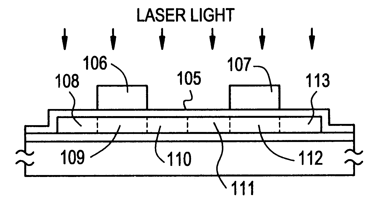
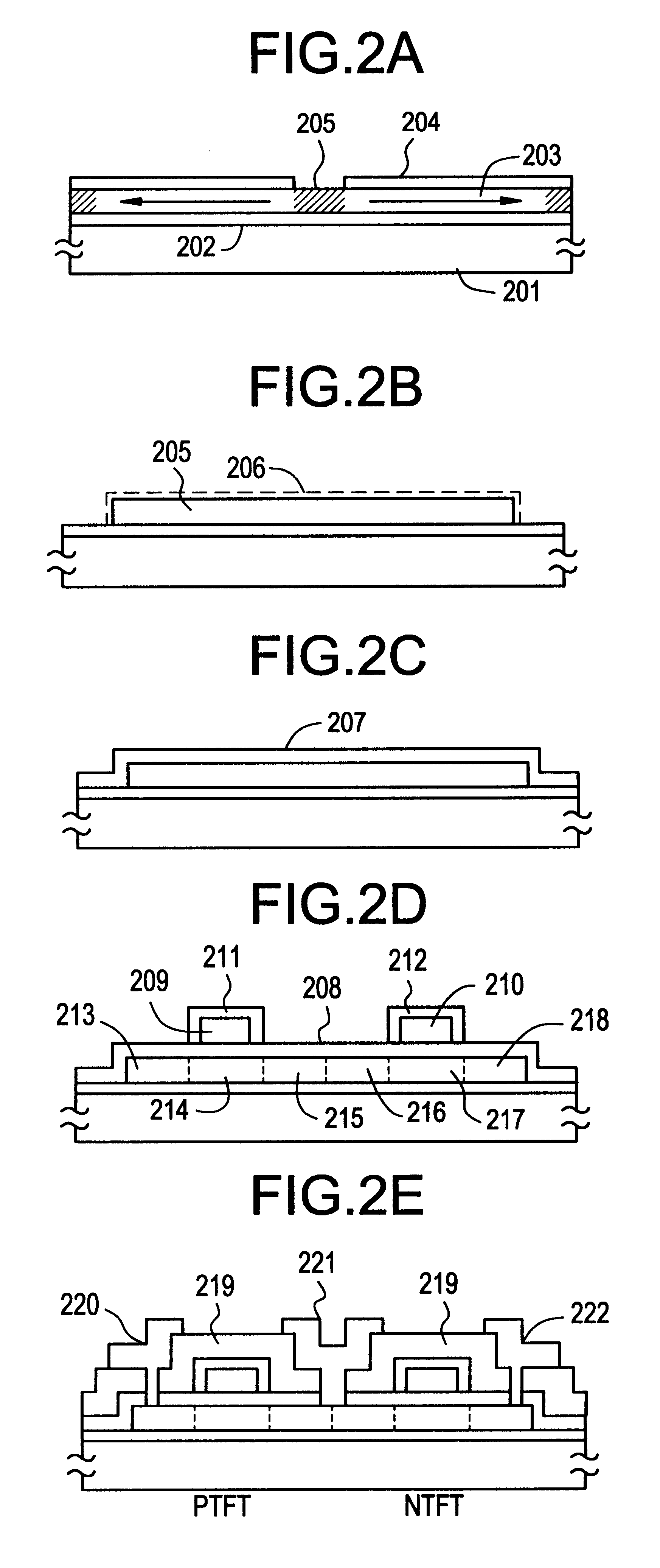
The present example refers to another complementary TFT circuit. Referring to FIG. 2, the present example is described in detail below. A Corning 7059 glass substrate 201 was annealed in the temperature range of from 620 to 660.degree. C. for a duration of 1 to 4 hours, gradually cooled at a rate of from 0.1 to 1.0.degree. C. / minute, preferably, at a rate of from 0.1 to 0.3.degree. C. / minute to a temperature in the range of from 450 to 590.degree. C., and was taken out from the heat treatment apparatus. A base film 202 was formed on the substrate thereafter, and an amorphous silicon film 203 was deposited at a thickness of from 300 to 800 .ANG. by plasma CVD. A nickel film from 20 to 50 .ANG. in thickness was deposited by sputtering in the region 205 using a silicon oxide mask 204 having a thickness of 1,000 .ANG.. The nickel film need not be a continuous film.

Then, the resulting structure was subjected to thermal annealing in a gaseous nitrogen atmosphere in the temperature range o...

example 3

FIGS. 5A-5G shows the step-sequential cross section structures obtained in the fabrication process according to the present example. A 2,000 .ANG. thick silicon oxide film was deposited as a base film 502 on a Corning 7059 glass substrate 501. The substrate was then annealed in the temperature range of from 620 to 660.degree. C. for a duration of 1 to 4 hours, gradually cooled at a rate of from 0.1 to 1.0.degree. C. / minute, preferably, at a rate of from 0.1 to 0.3.degree. C. / minute to a temperature in the range of from 450 to 590.degree. C., and was taken out from the heat treatment apparatus.

Then, a film of an intrinsic (I-type) amorphous silicon film was deposited by plasma-assisted CVD to a thickness of from 500 to 1,500 .ANG., for example, 1,000 .ANG.. The amorphous silicon film thus deposited was annealed for 48 hours at 600.degree. C. under a nitrogen inert gas atmosphere at the atmospheric pressure for crystallization. The silicon film thus obtained was then patterned to isl...

example 4

FIGS. 6A-6G show the step-sequential cross section structures obtained in the fabrication process according to the present example. A 2,000 .ANG. thick silicon oxide film was deposited as a base film 602 on a Corning 7059 glass substrate 601. The substrate was then annealed in the temperature range of from 620 to 660.degree. C. for a duration of 1 to 4 hours, gradually cooled at a rate of from 0.1 to 1.0.degree. C. / minute, preferably, at a rate of from 0.1 to 0.3.degree. C. / minute to a temperature in the range of from 450 to 590.degree. C., and was taken out from the heat treatment apparatus.

Then, a film of an intrinsic (I-type) amorphous silicon film was deposited by plasma-assisted CVD to a thickness of from 500 to 1,500 .ANG., for example, 1,000 .ANG.. The amorphous silicon film, thus deposited crystallized in the same manner as in Example 2 by using nickel as a catalyst. Thus, the crystallization was effected for a duration of 4 hours at 550.degree. C. under a gaseous nitrogen ...


PUM


Abstract

A method for manufacturing a semiconductor device comprises the steps of forming a semiconductor film on a substrate, oxidizing a surface of said semiconductor film in an oxidizing atmosphere with said semiconductor film heated or irradiated with light, and further depositing an oxide film on the oxidized surface of the semiconductor film by PVD or CVD. The first oxide film has a good interface condition with the semiconductor film and a characteristics of an insulated gate field effect transistor can be improved if the first oxide-film and the second oxide film are used as a gate insulating film.

Description

The present invention relates to a semiconductor device such as a thin film transistor (TFT) or a thin film diode (TFD), or a thin film integrated circuit (IC) to which TFT or TFD is applied, and in particular, a thin film integrated circuit (IC) for an active-matrix addressed (active matrix) liquid crystal display device, having an insulated gate structure comprising a semiconductor film provided on an insulating substrate such as a glass substrate, or on an insulating coating formed on any type of substrate. The present invention also relates to a process for fabricating the same.DESCRIPTION OF THE PRIOR ARTSemiconductor devices comprising TFTs on an insulating substrate (such as a glass substrate) developed heretofore include an active matrix-addressed liquid crystal display device using the TFTs for driving the matrices, an image sensor, and a three-dimensional IC.The TFTs utilized in those devices generally employ a thin film silicon semiconductor. Thin film semiconductors can ...

Claims


Application Information

Patent Timeline
IPC IPC(8): H01L21/336H01L21/02H01L21/28H01L29/49H01L21/70H01L29/40H01L27/12H01L21/84H01L29/45H01L21/77
CPCH01L21/28158H01L27/1214H01L29/4908H01L29/66757H01L29/458H01L27/1277
Inventor ADACHI, HIROKITAKENOUCHI, AKIRAFUKADA, TAKESHIUEHARA, HIROSHITAKEMURA, YASUHIKO
Owner SEMICON ENERGY LAB CO LTD
Why Eureka
Eureka Blog
Learn More