Thin film ferroelectric light modulators

a ferroelectric light and thin film technology, applied in the field of electro-optical modulators, can solve the problems of inconvenient production of large-scale hybrids, inconvenient manufacturing, and difficult production of hybrid integrated circuits

Inactive Publication Date: 2001-04-03
CORNING APPLIED TECH
View PDF32 Cites 30 Cited by
  • Summary
  • Abstract
  • Description
  • Claims
  • Application Information

AI Technical Summary

Problems solved by technology

Most of them are not suitable for producing useful large-scale hybrid, integrated-with-silicon, circuits.
All of these approaches have one major disadvantage.
Manufacturing may be costly and the need to make electrical contact to a vertical stack of electrodes may make it hard to produce as a hybrid integrated circuit.
Moreover, this device seems to be limited in useable angles of incidence.
This device can overcome the limitation on light wavelengths, but liquid crystal response times are inherently slow and PLZT was also proposed.
In this case, multiple reflections occur within the ITO layer itself and the overall structure is considerably more complicated than the case for a classical Fabry-Perot etalon.
This selection cannot always be accomplished in practice.
However, fortuitously, an ITO-PLZT-platinum combination produces a low enough minimum reflectance to be useful.
However, when a useful thickness of platinum is used for the bottom mirror / electrode, the light will be absorbed by it.)

Method used


Image

  • Thin film ferroelectric light modulators
  • Thin film ferroelectric light modulators
  • Thin film ferroelectric light modulators

Examples


##ic example # 1

PROPHETIC EXAMPLE #1

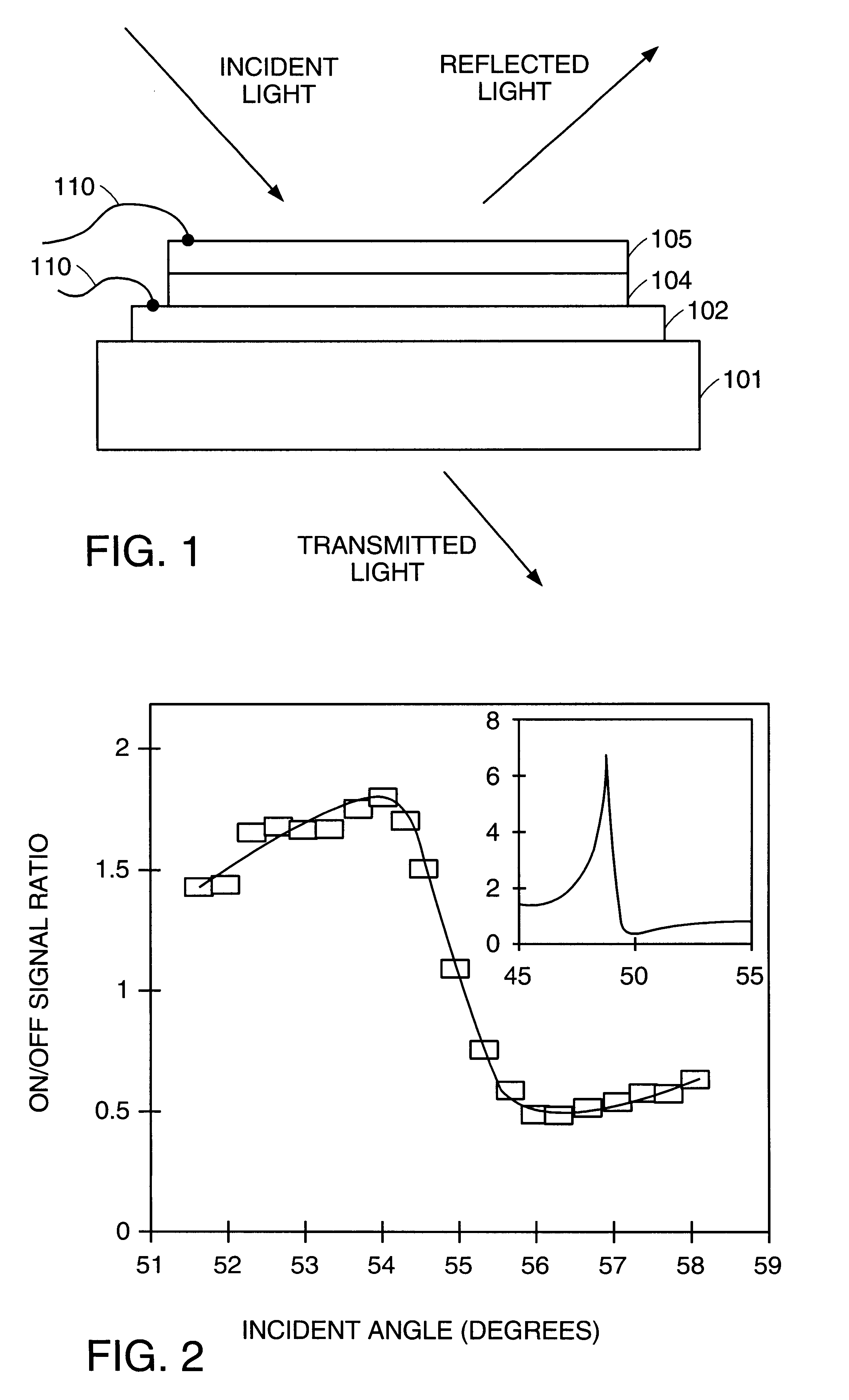
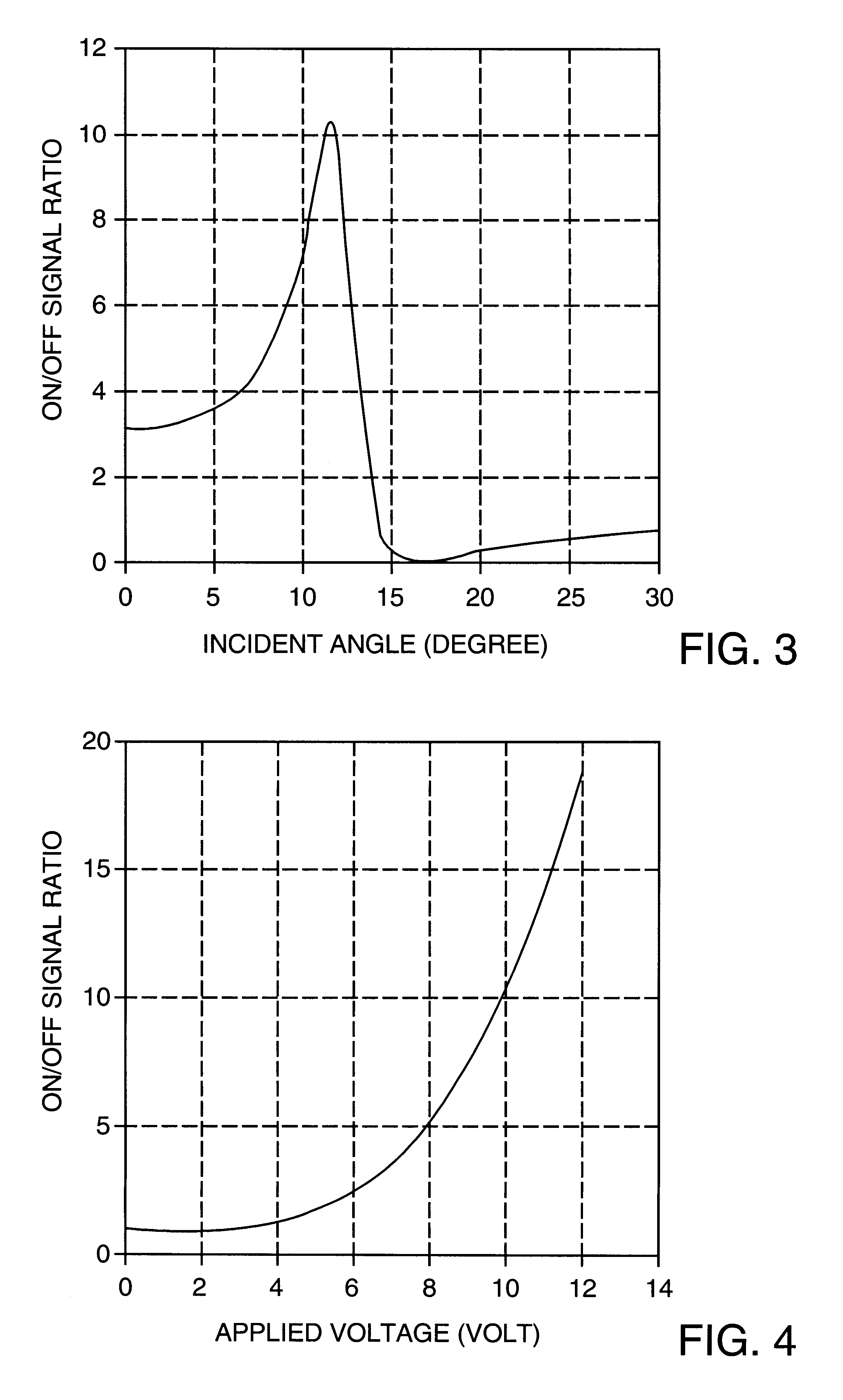
As the angle of the incident light approaches the normal to the structure, the difference between s and p-wave reflections approaches zero. In this case, one may use totally unpolarized light and still obtain a high ratio of on and off signals. FIG. 3 shows a theoretical calculation for small angles for unpolarized light with a 10 volt modulation voltage applied to the ferroelectric. This was for an ITO thickness of 0.25 wavelengths and a PLZT thickness of 1.278 wavelengths of the light. In general, using equation (1), an optimum thickness can be determined for the ITO and PLZT layers for any given incident angle and wavelength. The major limitation on the on / off ratio is the minimum off intensity which depends on how closely one can satisfy equation (3).

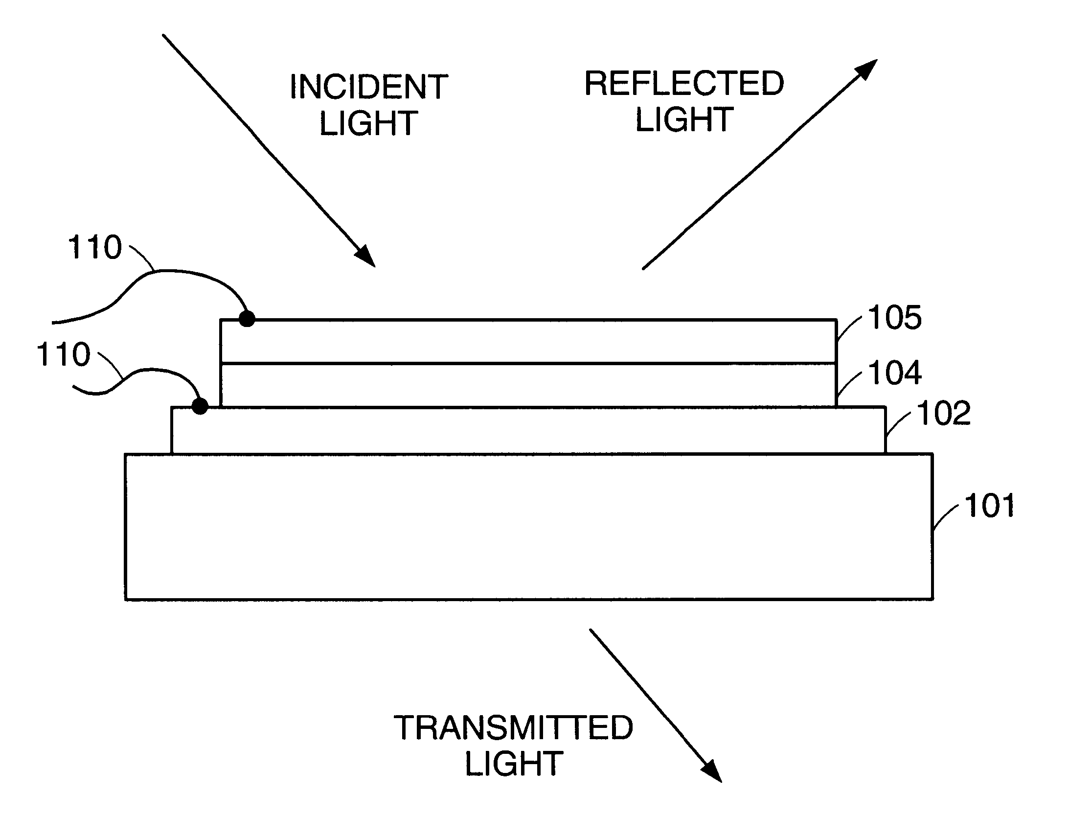
Even though the modulator is not bistable but produces continuous modulation with applied voltage, it is convenient to measure modulation as the ratio of reflectance when some fixed voltage is applied and none. F...

working example # 2

WORKING EXAMPLE #2

A device was constructed as illustrated in FIG. 5 wherein the bottom mirror / electrode 102 of FIG. 1 was comprised of a dielectric mirror 202 and conductive transparent layer of ITO 203. The use of a stack of layers of alternating index of refraction material to produce nearly perfect mirrors at selected wavelengths is well known, but producing crystalline thin film oxide ferroelectrics on such a dielectric mirror is believed to be unknown.

PLZT thin films can be made by a variety of methods. In this working example, one was made using the Metalorganic Chemical Liquid Deposition (MOCLD) process, K. K. Li, G. H. Haertling and W. -Y. Howng, "An Automatic Dip Coating Process for Dielectric Thin and Thick Films," Integrated Ferroelectrics, vol. 3, pp 81-91 (1993). Dip coating is an old art used for a variety of materials. As described in this reference for PLZT, a solution of acetate precursors of the constituents is prepared and a substrate is dipped, withdrawn, allowed...

##ic example # 2

PROPHETIC EXAMPLE #2

As noted above, using a dielectric stack for the top mirror function as well as the bottom one, as shown in FIG. 7, should result in a major improvement over using gold for the top mirror / electrode. The figure illustrates a substrate 101, a bottom dielectric stack 202, a bottom transparent electrode 203, a ferroelectric film 104, a top transparent electrode 305, and a top dielectric stack 306. Alternating SiO.sub.2 and Ta.sub.2 O.sub.5 layers could be used for the top dielectric stack 306 as well as the bottom 202, but, since the ferroelectric film 204 is formed first, high temperature materials are not required for the top stack 306 and others may be more convenient.

As is well known, the reflectivity of a dielectric stack increases with the number of layers in a predictable manner. In this calculation, enough were chosen so that, coupled with the ITO electrodes, the combination possessed a reflectivity of 98.9%. Using such a combination for both the top and bott...


PUM

PropertyMeasurementUnit
reflectivityaaaaaaaaaa
thickaaaaaaaaaa
thickaaaaaaaaaa

Abstract

A solid state device used to modulate the intensity of reflected or transmitted light by modulating with an external voltage the optical thickness of a thin film ferroelectric placed in an etalon cavity is disclosed. The device is constructed by selecting a generally planar supporting substrate, preferably silicon or sapphire in order to be compatible with silicon integrated circuits. A dielectric stack consisting of alternating layers of different index of refraction materials, also specifically selected to be compatible with later growth of the thin film ferroelectric, is deposited thereon to form a partially reflective and partially transmitting mirror, followed by a transparent electrically conductive layer. The thin film ferroelectric is deposited on the conductive layer, followed by a second transparent conductive layer and a second dielectric stack. Leads are connected to the conductive layers and in turn to a voltage generator. In one version of the invention, the functions of both the second (top) electrically conductive layer and dielectric stack are fulfilled by using a semi-transparent conducting film. In another version, the functions of both the first (bottom) electrically conductive layer and dielectric stack are also fulfilled by using a, preferably, highly reflective conducting film.

Description

1. Technical FieldThe invention is in the field of electro-optic modulators of light wave intensity. More particularly, the invention relates to using thin film ferroelectric materials in a Fabry-Perot etalon to provide polarization-insensitive modulation of reflected and transmitted light at high modulation frequencies.2. Related ArtA number of methods or devices have been proposed to modulate the intensity of light. Most of them are not suitable for producing useful large-scale hybrid, integrated-with-silicon, circuits. The closest related art to the present invention uses ferroelectric materials whose indices of refraction change when an electric field is applied, but at a different rate for different light polarizations. That is, the ordinary and the extraordinary index change at a different rate with applied voltage, i.e., a field induced birefringence occurs. This structure is similar to an asymmetric Fabry-Perot etalon with a back surface reflecting electrode and a front surf...

Claims


Application Information

Patent Timeline
Patent Type & Authority Patents(United States)
IPC IPC(8): G02F1/01G02F1/21G02F1/19G02F1/055
CPCG02F1/21G02F1/19G02F1/055Y10T428/24942G02F2201/307
Inventor WANG, FEILINGHAERTLING, GENE H.
Owner CORNING APPLIED TECH
Why Eureka
Try Eureka