Method for forming an insulating film on semiconductor substrate surface and apparatus for carrying out the method

a technology of insulating film and semiconductor substrate, which is applied in the direction of electrical equipment, semiconductor devices, electric discharge tubes, etc., can solve the problems of insufficient improvement of silicon dioxide film quality, small amount of nitrogen atoms incorporated into the formed oxynitride film, and failure to form thin high-quality oxynitride films with good controllability and reproducibility. , to achieve the effect of good controllability, good controllability, and efficient operation

Inactive Publication Date: 2001-07-24
JAPAN SCI & TECH CORP +1
View PDF12 Cites 121 Cited by
  • Summary
  • Abstract
  • Description
  • Claims
  • Application Information

AI Technical Summary

Benefits of technology

According to the above-mentioned method of the present invention, an insulating film having a thickness of 1-20 nm is deposited on a semiconductor substrate. Subsequently, the thus-deposited insulating film is exposed to plasma generated by electron impact while semiconductor substrate temperature is maintained at 700.degree. C. or lower. As a result, an insulating film having uniformly high quality can be formed on a semiconductor substrate in an efficient, rational manner and with good controllability.

Problems solved by technology

However, these methods fail to form thin high-quality oxynitride films with good controllability and reproducibility.
Conventionally practiced thermal oxynitridation using N.sub.2 O gas has involved the following problems: heating at high temperatures is required; the amount of nitrogen atoms incorporated into a formed oxynitride film is relatively small; and the quality of a silicon dioxide film is not sufficiently improved.
According to conventionally practiced thermal oxynitridation using NO gas, a heating temperature is as low as about 900.degree. C., and the amount of nitrogen atoms incorporated into a formed oxynitride film increases somewhat; however, the method has involved the problem that the thickness of a formed oxynitride film cannot be made greater than a certain level.
A formed oxynitride film contains a large amount of hydrogen, which serves as an electron trap, causing an impairment in film quality.
Also, conventionally practiced direct oxynitridation using plasma has involved the problem that film quality is impaired due to plasma damage.
Particularly, the generation of interface state not only impairs hot-carrier properties of a transistor but also causes an unstable threshold voltage of a transistor and impaired mobility of carriers, which induce a fatal problem for, particularly, fine-patterned devices.
Accordingly, high-temperature heating has raised the problems of dopant diffusion and defect generation.
As a result, impairment in film quality is involved.
Also, the use of N.sub.2 plasma has involved insufficient improvement of film quality, since the amount of nitrogen atoms incorporated into a film is relatively small.

Method used


Image

  • Method for forming an insulating film on semiconductor substrate surface and apparatus for carrying out the method
  • Method for forming an insulating film on semiconductor substrate surface and apparatus for carrying out the method
  • Method for forming an insulating film on semiconductor substrate surface and apparatus for carrying out the method

Examples


first embodiment

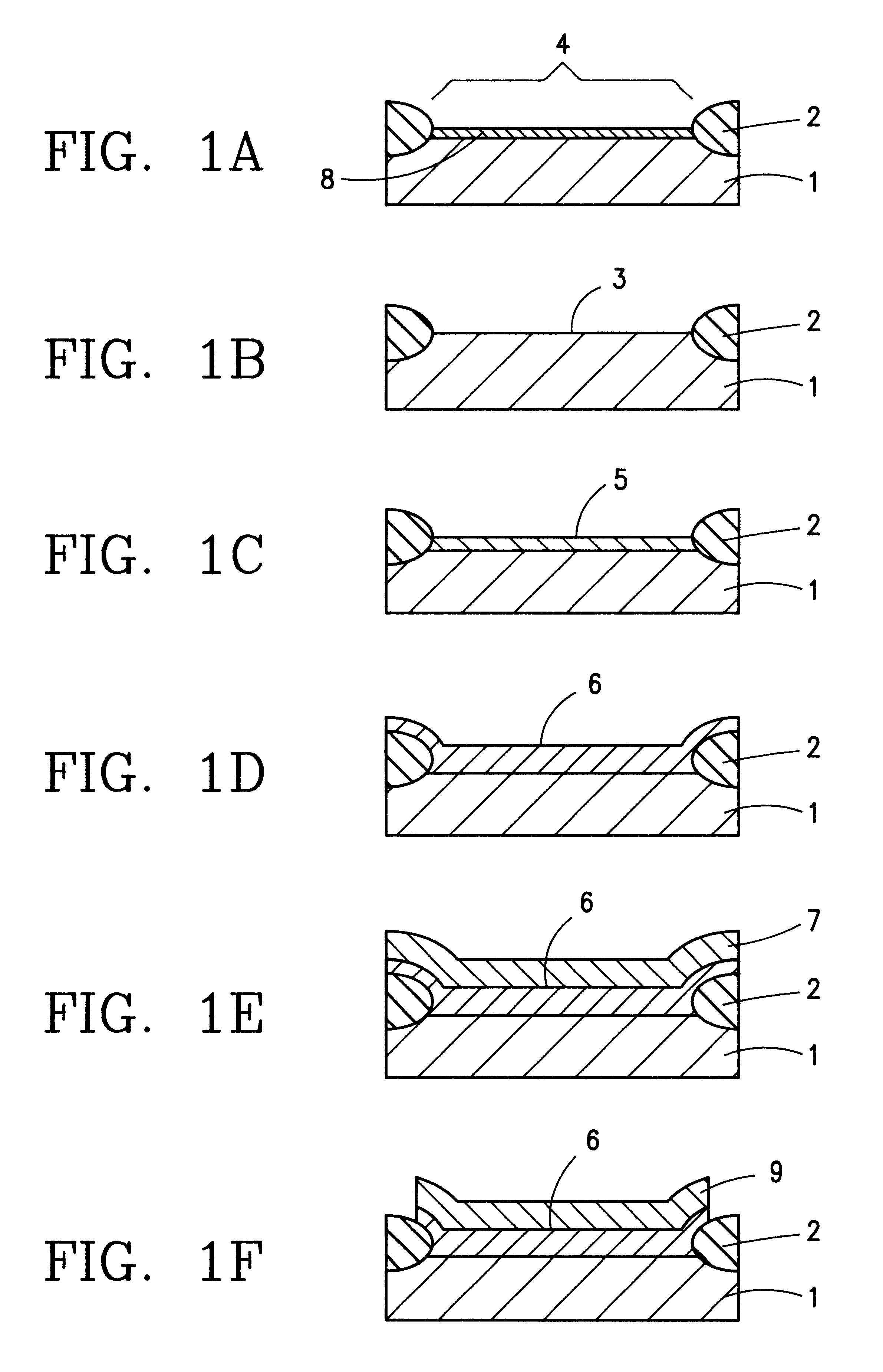
FIGS. 1A to 1F show a process of forming an insulating film on a semiconductor substrate according to the present invention. In the present embodiment, an MOS capacitor is formed on a silicon substrate, which is an example of the semiconductor substrate.

(1) An isolation region 2 and an active region 4 were formed on a silicon substrate 1 through use of a known selective oxidation technique. A native oxide film 8 was present on the surface of the active region 4 (FIG. 1A). Specifically, the silicon substrate 1 was a p-type (100) substrate having a resistivity of 10-15 .OMEGA.cm. The isolation region 2 was an LOCOS (local oxidation of silicon) oxide film having a thickness of 500 nm.

(2) In order to clean the active region 4, a wafer was cleaned by a known RCA cleaning method (W. Kern, D. A. Plutien: RCA Review, 31, pp. 187, 1970). Subsequently, the wafer was immersed in a dilute HF solution (0.5 vol. % aqueous solution of HF) for 5 minutes, thereby removing the native oxide film 8 fro...

second embodiment

Next, the present invention will be described.

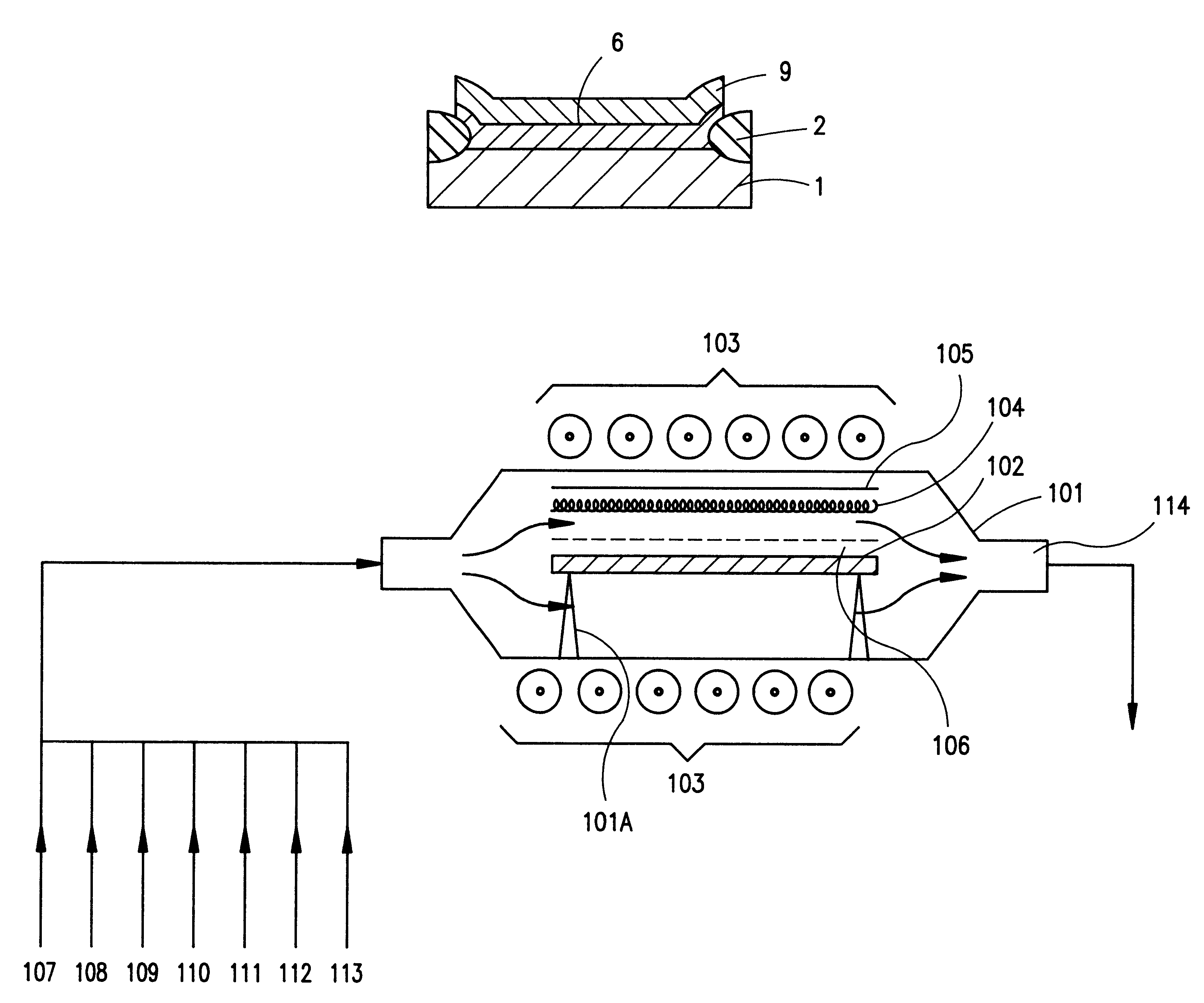
FIG. 10 shows a schematic configuration of an apparatus for forming an insulating film on the surface of a semiconductor substrate.

As shown in FIG. 10, in a horizontally elongated chamber 101, a semiconductor substrate 102 is supported horizontally on support pins 101A. The chamber 101 is formed of stainless steel SUS 316 and has a volume of about 18000 cm.sup.3.

A thermoelectron source (tungsten filament) 104, a grid electrode 105, and a mesh electrode 106 are provided at an upper portion of the chamber 101. A voltage can be applied to both ends of the filament 104 so as to heat the filament 104 in order to release thermoelectrons from the heated filament 104. A voltage can be applied to the grid electron 105 so as to accelerate thermoelectrons released from the filament 104.

A voltage can also be applied to the mesh electrode 106 and the semiconductor substrate 102. Through adjustment of the applied voltages, incident charge on the surfa...


PUM

PropertyMeasurementUnit
thicknessaaaaaaaaaa
temperatureaaaaaaaaaa

Abstract

Disclosed are a method and apparatus for forming an insulating film on the surface of a semiconductor substrate capable of improving the quality and electrical properties of the insulating film with no employment of high-temperature heating and with good controllability. After the surface of a silicon substrate is cleaned, a silicon dioxide film having a thickness of 1-20 nm is formed on the substrate surface. The silicon substrate is exposed to plasma generated by electron impact, while the silicon substrate is maintained at a temperature of 0° C. to 700° C. Thus, nitrogen atoms are incorporated into the silicon dioxide film, obtaining a modified insulating film having good electrical properties.

Description

1. Field of the InventionThe present invention relates to a method for forming an insulating film on the surface of a semiconductor substrate and to an apparatus for carrying out the method.2. Description of the Related ArtConventionally, silicon oxynitride films are used as gate insulation films and capacitor insulating films for semiconductor devices, particularly, when they are silicon devices, MOS (Metal Oxide Semiconductor) transistors and MOS capacitors. These insulating films must have a high dielectric breakdown voltage and a high dielectric breakdown charge amount. A wafer cleaning process plays an important role in attainment of the requirement, as wafers must be properly cleaned and have a low fixed electric charge density and a low interface state density.Along with a recent tendency to reduce the geometry and increase integration of semiconductor device circuits, gate insulating films and capacitor insulating films are becoming thinner. For example, under the design rul...

Claims


Application Information

Patent Timeline
Patent Type & Authority Patents(United States)
IPC IPC(8): H01L21/02H01L21/314H01L21/31H01L21/316H01L21/318H01L29/78
CPCH01L21/3144H01L21/28202H01J2237/3387Y10S438/961H01L21/02236H01L21/0214H01L21/02271H01L21/02266H01L21/02238H01L21/02241H01L21/02274H01L21/02255H01L21/31H01L21/0234H01L21/02332
Inventor KOBAYASHI, HIKARUYONEDA, KENJI
Owner JAPAN SCI & TECH CORP
Why Eureka
Try Eureka