Frequency selected, variable output inductor heater system

a heater system and variable output technology, applied in the direction of chemically reactive gases, crystal growth process, electric/magnetic/electromagnetic heating, etc., can solve the problem of significant temperature differences, non-uniform thickness layer on the wafer, ineffective in minimizing the temperature gradient across the surface of the wafer, etc. problem, to achieve the effect of rapid temperature changes

Inactive Publication Date: 2001-11-13
ADVANCED ENERGY IND INC
View PDF5 Cites 32 Cited by
  • Summary
  • Abstract
  • Description
  • Claims
  • Application Information

AI Technical Summary

Benefits of technology

It is yet a further object of the invention to permit rapid temperature changes in an object being heated by an induction heating system while simultaneously holding the temperatures of a plurality of zones of said object precisely equal.
It is a further object of the present invention to maintain the temperatures of a plurality of zones of said object in exact proportion to one another as the object is cooled from a heated state.

Problems solved by technology

One of the problems in forming layers of materials on a semiconductor wafer is ensuring that the temperature of the semiconductor wafer is kept uniform across the wafer during the deposition process, i.e., during heat-up, processing, and cool-down.
Since the deposition rate of a layer of material upon the wafer is dependent on the temperature of the wafer, any temperature variations between the center and edge of a wafer will undesirably result in the deposition of a layer of non-uniform thickness on the wafer.
In addition, non-uniform temperatures during heat-up, processing, and cool-down can cause stress on the wafer, undesirably resulting in slip.
However, since heat loss is typically greater at the edge of a wafer than at the center, such earlier systems may result in significant temperature differences between the center and outer portions of the wafer and, thus, may be largely ineffective in minimizing temperature gradient across the surface of a wafer.
Each of these lamps, which is typically of the tungsten halogen type, has a finite useful life and thus must be periodically replaced.
The replacement of such lamps, as well as the periodic adjustment of the lamps due to their aging, not only increases manufacturing cost but also decreases the throughput of the chemical vapor deposition (CVD) system.
Furthermore, the use of such heating lamps in a radiantly heated CVD system undesirably requires periodically cleaning of the quartz walls of the reaction chamber to remove deposited material from the chamber walls.
Since the entire cycle in warm wall CVD systems may be between five and ten minutes, cleaning the walls accounts for a significant portion of the total cycle time and, therefore, can severely reduce throughput of the CVD system.

Method used


Image

  • Frequency selected, variable output inductor heater system
  • Frequency selected, variable output inductor heater system
  • Frequency selected, variable output inductor heater system

Examples


Embodiment Construction

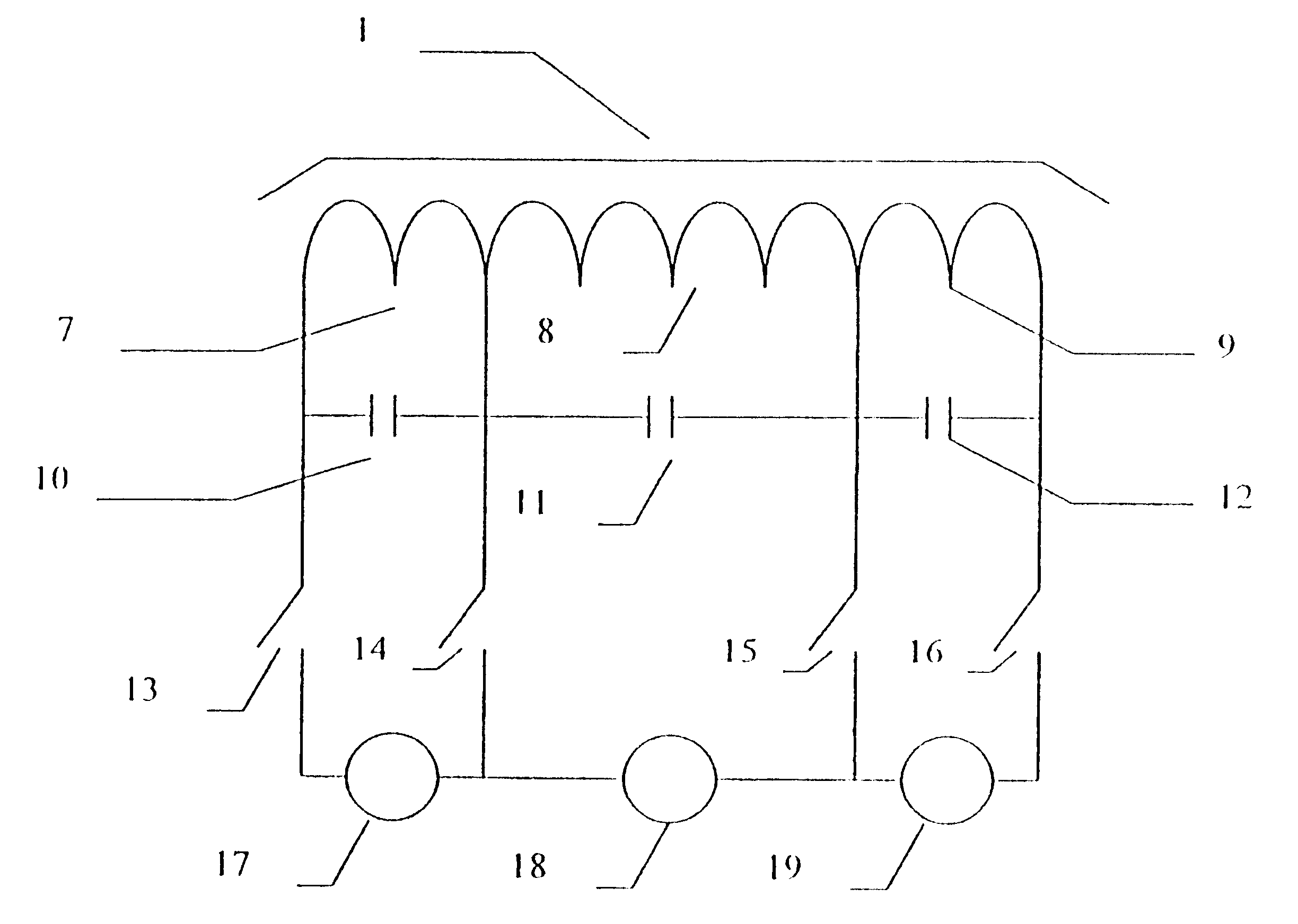
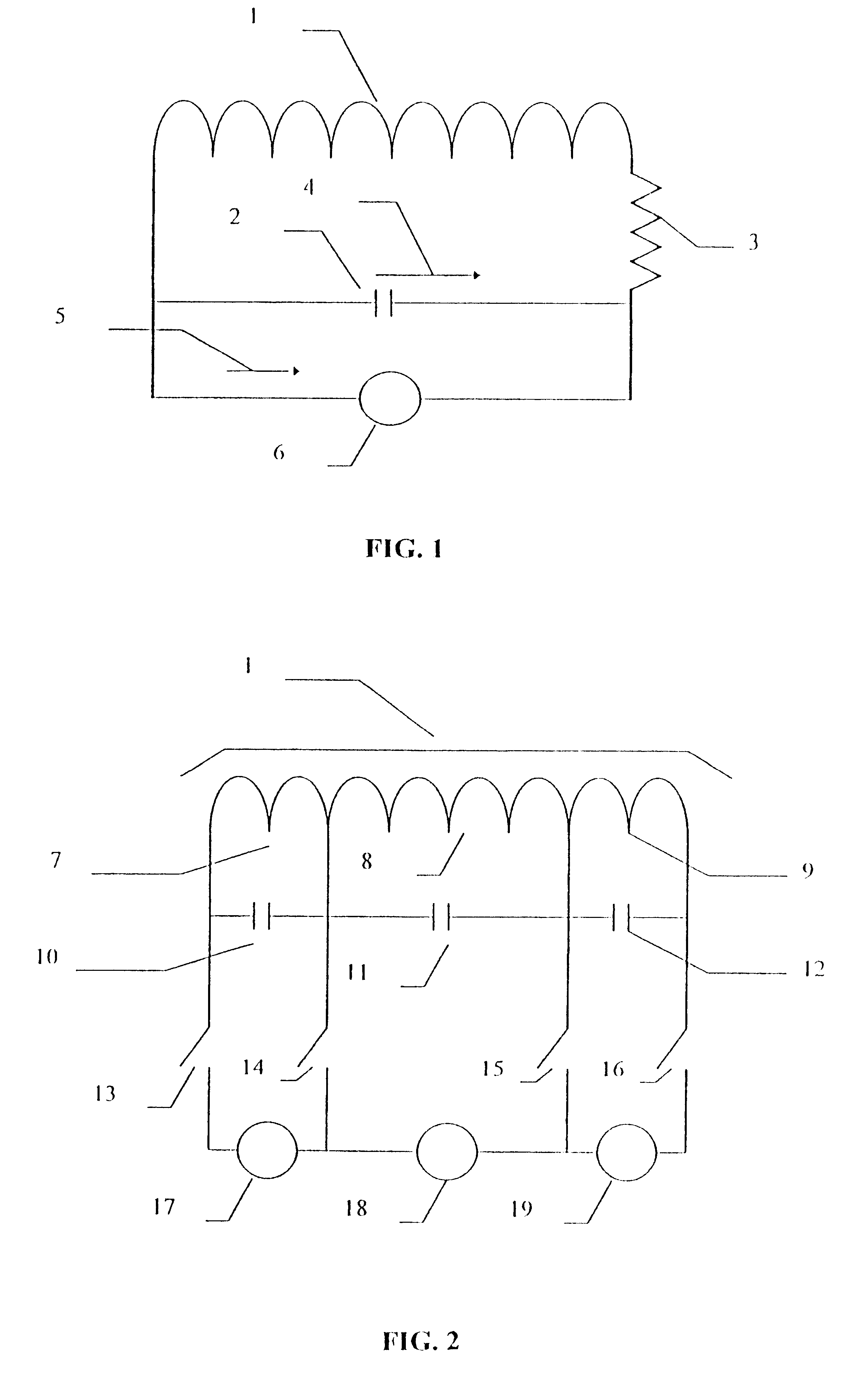
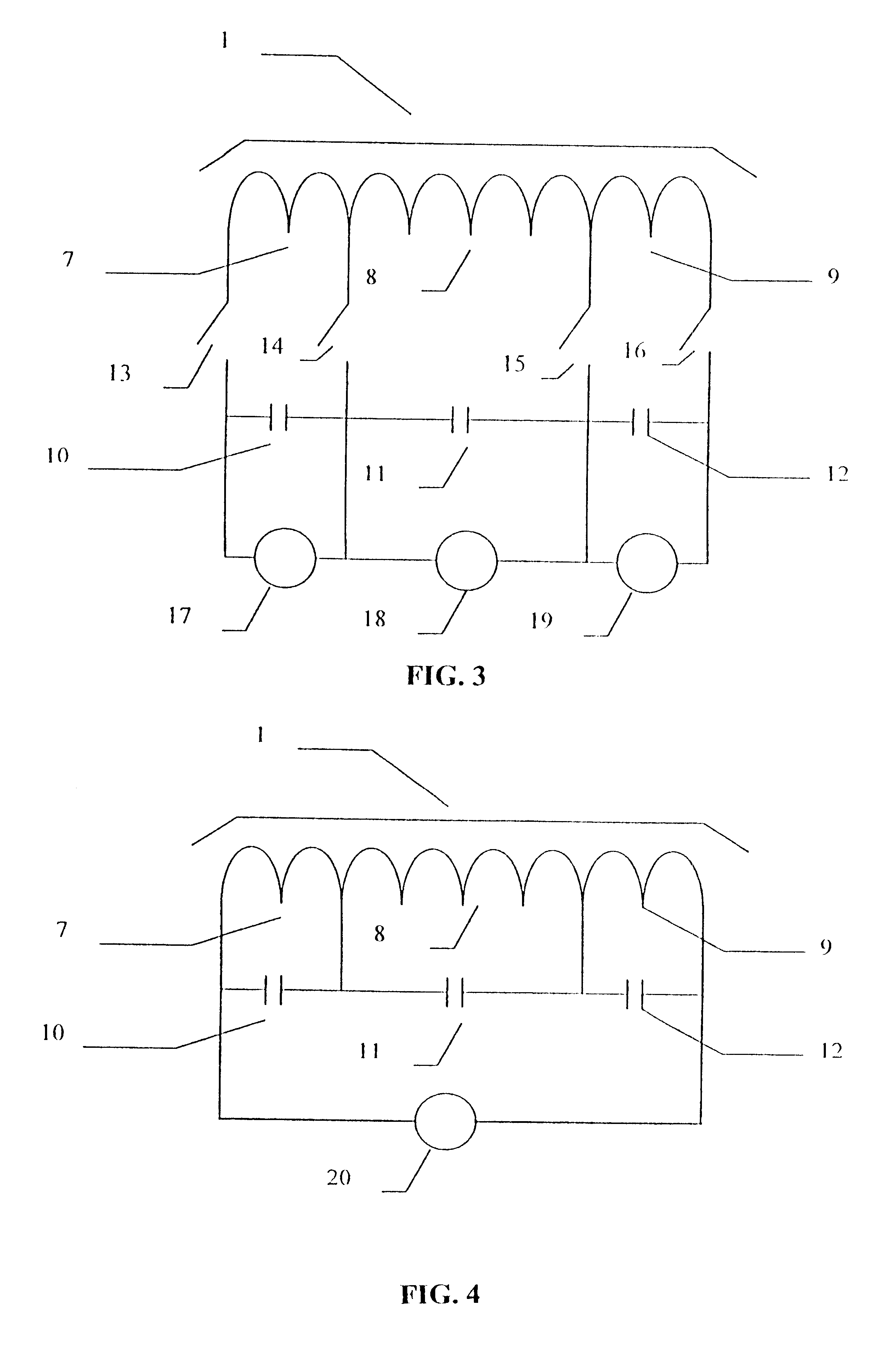
In general, an induction heating system is comprised of a power supply, an induction coil, an object to be heated and, if necessary, a "susceptor" to absorb energy from the magnetic field of the coil and retransmit that energy to the object to be heated. The system operates on the principle of induction of circulating currents in the object to be heated or the susceptor, if present. Generally a susceptor is used if the object to be heated is not adequately conductive (and thus cannot support the induced heating currents) or would be damaged in some way by such currents. The currents required to obtain substantial heating in large objects or rapid heating of small objects are large. A coil carrying large currents creates a large magnetic field in its vicinity, and energy is stored in this field. While much of the field may be canceled by the induced current in the susceptor or object to be heated, there remains enough to store appreciable energy. This energy is represented electrical...


PUM

PropertyMeasurementUnit
temperatureaaaaaaaaaa
electrical resonance frequencyaaaaaaaaaa
resonance frequenciesaaaaaaaaaa

Abstract

An induction heating systems using a plurality of zones in a coil provides selective heating control for better uniformity especially for semiconductor and other thin film processing applications. By arranging the zones to have different resonance frequencies, the power supply may control the various zones by altering its frequency output. The power supply may also act to control the differential heating by switching among zones in conjunction with the frequency control, by sweeping through a variety of frequencies, by simultaneously providing power over different frequencies, by altering the residence time at each frequency, or by outputting different powers to each frequency or the like. Each zone may thus be tuned as appropriate to achieve the desired induction heating characteristic.

Description

This invention relates to heating systems using high frequency energy to induce currents in objects to heat them directly or indirectly ("induction heating systems"). In particular it relates to heating systems for semiconductor processing equipment in which layers are formed on heated semiconductor wafers by Chemical Vapor Deposition.Equipment for the formation of layers, such as epitaxial silicon or polysilicon, on semiconductor wafers is well known. One of the problems in forming layers of materials on a semiconductor wafer is ensuring that the temperature of the semiconductor wafer is kept uniform across the wafer during the deposition process, i.e., during heat-up, processing, and cool-down. Since the deposition rate of a layer of material upon the wafer is dependent on the temperature of the wafer, any temperature variations between the center and edge of a wafer will undesirably result in the deposition of a layer of non-uniform thickness on the wafer. In addition, non-unifor...

Claims


Application Information

Patent Timeline
Patent Type & Authority Patents(United States)
IPC IPC(8): C30B25/10H01L21/205C23C16/46H01L21/00H05B6/06H05B6/44
CPCC23C16/46C30B25/10H01L21/67109H05B6/06H05B6/44
Inventor SCHATZ, DOUGLAS S.DORRENBACHER, JOHN M.
Owner ADVANCED ENERGY IND INC
Why Eureka
Try Eureka