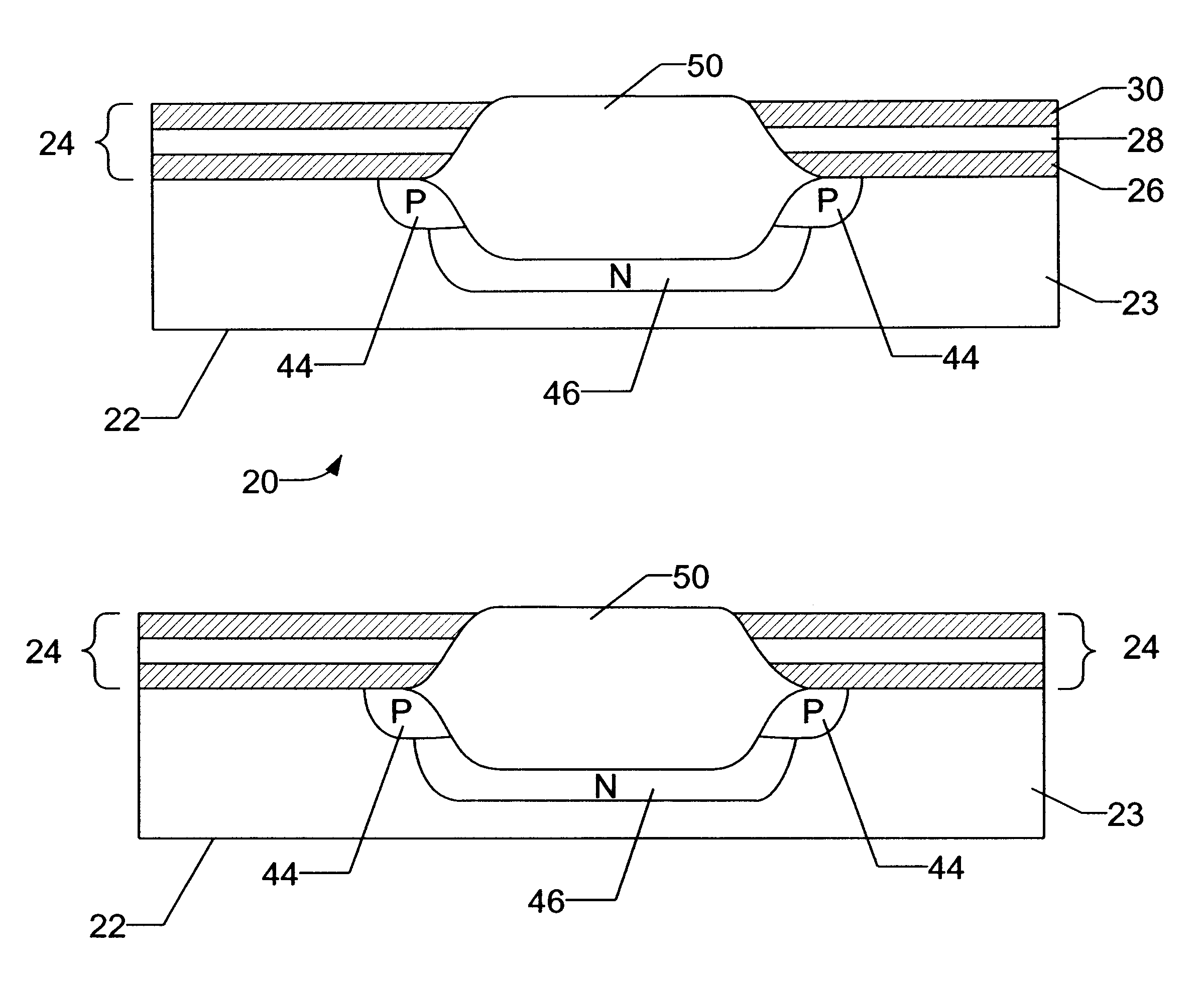
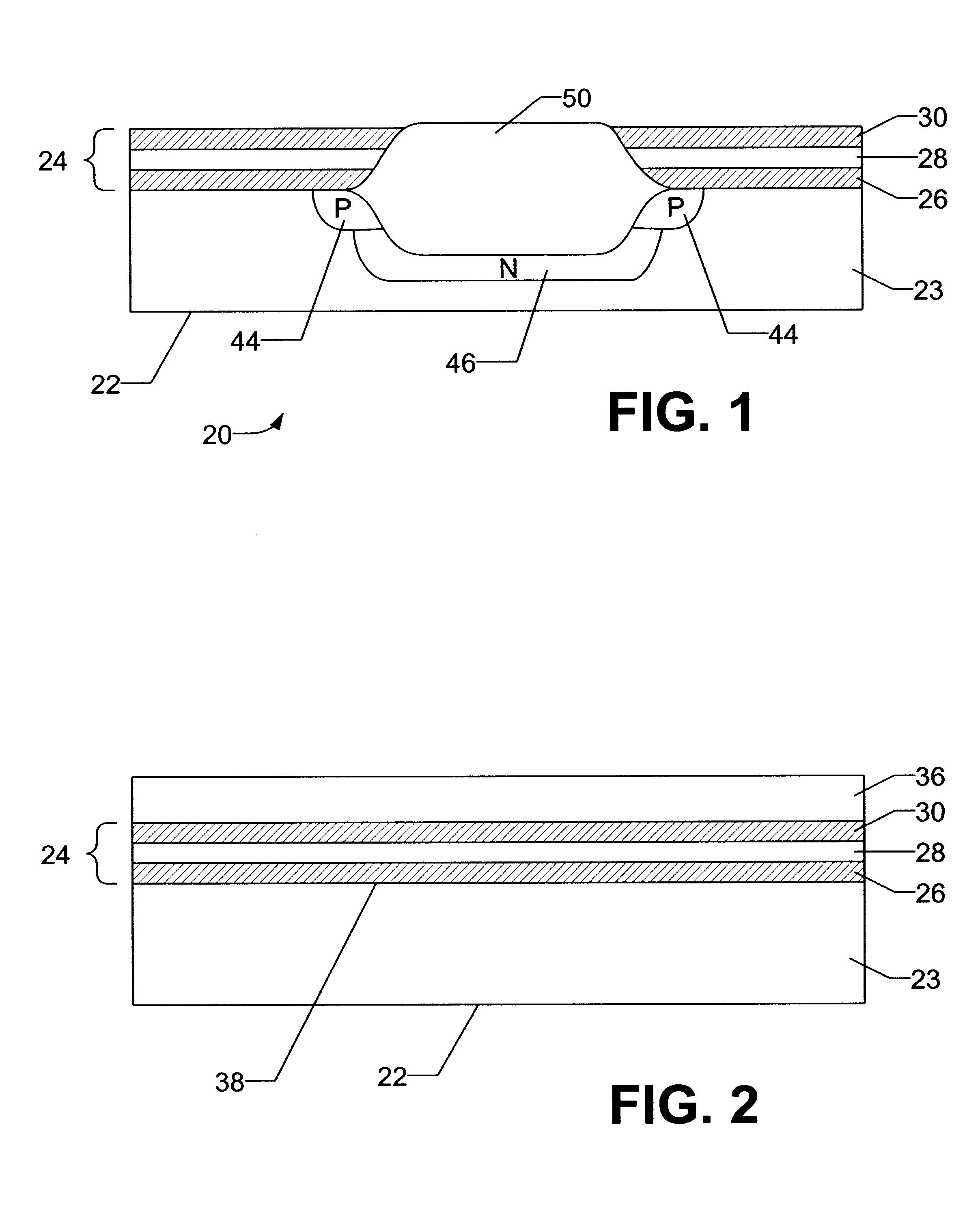
The present invention is for a process for fabricating a
memory cell in a non-volatile memory device, preferably in a two-bit EEPROM device. Fabrication of a two-bit EEPROM device having a
memory cell requires the formation of p-type regions and n-type regions with good
critical dimension control. This is because proper functionality of the two-bit EEPROM device during a
programming operation requires voltages to be applied to the p-type regions and n-type regions. In particular, the p-type regions must be positioned at the edges of the ONO layer for fabrication of
high density devices. However, fabrication of
high density devices with p-type regions positioned at the edges of the ONO layer is hard to obtain due to the limitations of the resist mask. By reducing the thickness of the resist mask and
rounding the edges of the resist mask, a high-density two-bit EEPROM device with good critical dimensions control can be manufactured.
In one form, a process for fabricating a memory
cell includes providing a semiconductor substrate and forming an ONO layer over the semiconductor substrate. A layer of
photoresist is then deposited overlying the ONO layer and patterned into a resist mask. The resist mask is thick enough to withstand an n-type
implant. The semiconductor substrate is then doped with an n-type
dopant such as
arsenic, preferably by using
ion implantation. The
doping of the semiconductor substrate with an n-type dopant causes n-type regions to form in the semiconductor substrate. Preferably, the n-type
implant is a direct implant, which is an implant at an angle substantially normal with respect to the principal surface of the semiconductor surface. After
doping the semiconductor substrate with n-type dopants, the resist mask is then etched to reduce the thickness of the resist mask and round the edges of the resist mask. Once the resist mask is etched, the semiconductor substrate is doped with p-type dopants such as
boron, preferably by using
ion implantation. The p-type implant is an angled implant, which is an implant at an angle substantially acute with respect to the principal surface of the semiconductor substrate. The
doping of the semiconductor substrate with p-type dopants causes p-type regions to form in the semiconductor substrate. After doping the semiconductor substrate with p-type dopants, the resist mask is removed and the bit-line
oxide region is formed. The rounded edges and reduced thickness of the resist mask allow for a more angled implant. The more angled implant allows for the fabrication of a memory
cell with tighter critical dimensions. In one preferred embodiment, the resist mask is etched to reduce the thickness of the resist mask and round the edges of the resist mask, before the doping the semiconductor substrate with n-type dopants and p-type dopants.
Photoresist layer 36 must be thick enough to withstand the doping of semiconductor substrate 22 with n-type dopants. Preferably,
photoresist layer 36 has a thickness of about 4,000 to about 10,000 angstroms and, more preferably, a thickness of about 5,000-6,000 angstroms. After
photoresist 36 has been deposited, photoresist layer 36 is patterned into resist mask 34, as illustrated in FIG. 3. Preferably, photoresist layer 36 is exposed to a
light source, such as an ultra-
violet light source, which allows for the patterning of photoresist layer 36 into resist mask 34.
Resist mask 34 has sharp edges 35, as illustrated in FIG. 3.
Once photoresist layer 36 has been patterned, semiconductor substrate 22 is then doped with an n-type dopant using resist mask 34 as a doping mask. Preferably, n-type dopant comprises an element selected from the group consisting of
antimony,
arsenic, and
phosphorus. Preferably, semiconductor substrate 22 is doped with
arsenic. In one preferred embodiment of this invention, the semiconductor substrate 22 is doped with an n-type dopant, such as arsenic, by using
ion implantation.
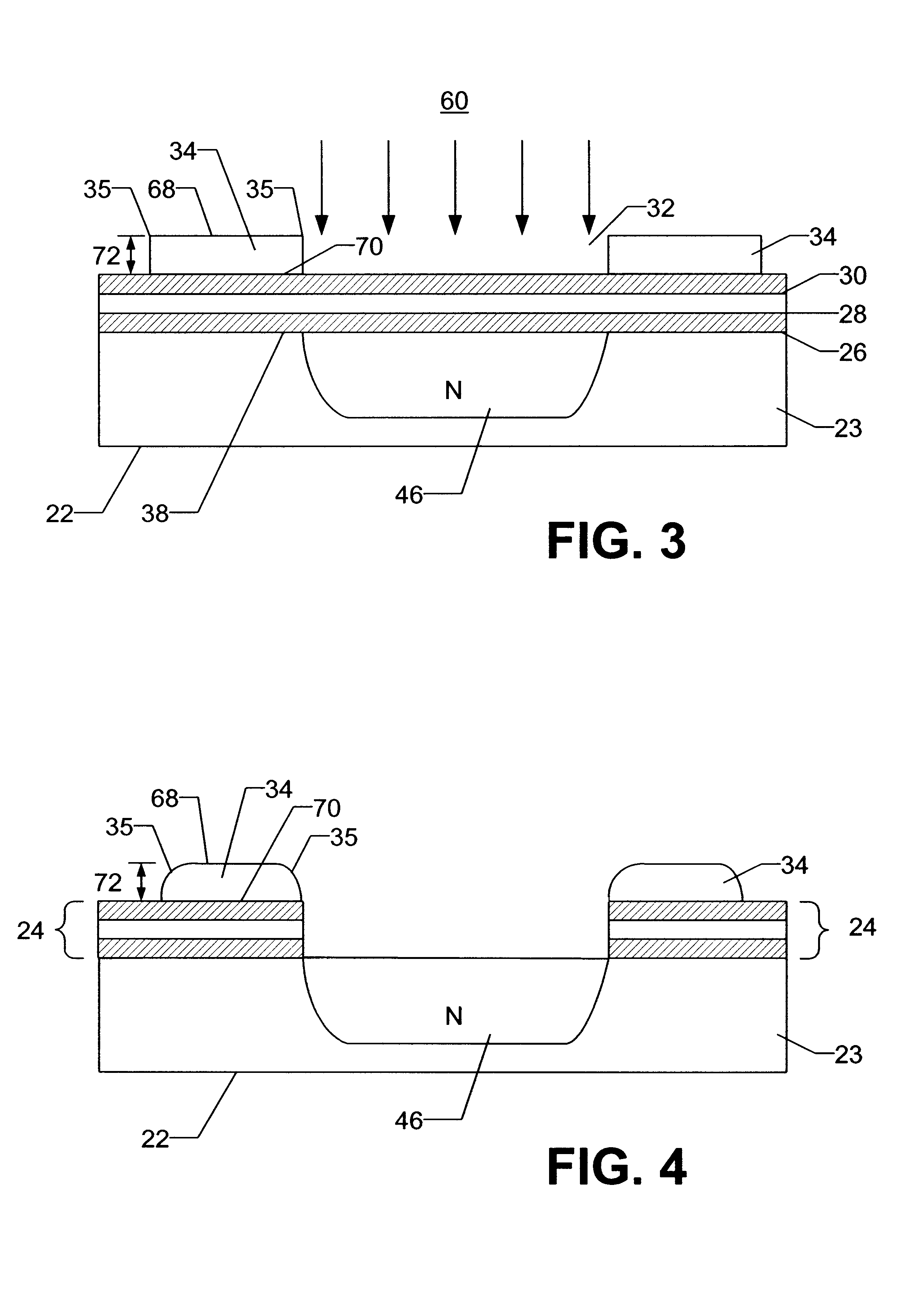
Ion implantation allows for the fabrication of memory
cell 20 with higher density and smaller feature sizes. Using resist mask 34 as an ion implant mask, n-type implant 60 is then performed, as illustrated in FIG. 3. The n-type implant 60 is preferably arsenic implanted at a
dose of about 1.times.10.sup.14 cm.sup.-2 to about 1.times.10.sup.16 cm.sup.-2 at an implant energy of about 20 KeV to about 80 KeV. Preferably, n-type implant 60 is performed through Ad ONO layer 24, but is masked out by resist mask 34, as illustrated in FIG. 3. The n-type implant is preferably a direct implant performed at an angle substantially normal to the principal surface 38 of the semiconductor substrate 22, such as about a 90.degree. angle, as illustrated in FIG. 3. The n-type implant 60 provides a high
breakdown voltage for the drain node, which is needed during cell erasure. The n-type implant 60 also forms the buried bit-line, which is a sub-surface
conductive channel that carries a
signal to each bit in the memory cell 20.
Applying an etch to resist mask 34 thins down resist mask 34 and causes edges 35 of resist mask 34 to become rounded. The rounded edges 35 and thinness of resist mask 34 allow for a more angled p-type implant 62, as illustrated in FIG. 5. The more angled implant allows for the fabrication of a memory cell 20 with tighter critical dimensions. In one preferred embodiment, an etch is applied to the exposed ONO layer 24 to
expose part of semiconductor substrate 22, as illustrated in FIG. 4. Preferably, the etch applied to
expose part of semiconductor substrate 22 is applied after the n-type implant 60 is performed.

