

Method of manufacturing epitaxial wafer
a manufacturing method and technology of epitaxial wafer, applied in the direction of crystal growth process, polycrystalline material growth, chemically reactive gas growth, etc., can solve the problems of increasing leakage current, increasing leakage current, and shortening the life of the carrier,
- Summary
- Abstract
- Description
- Claims
- Application Information
AI Technical Summary
Benefits of technology
Problems solved by technology
Method used
Image

Examples
example 1
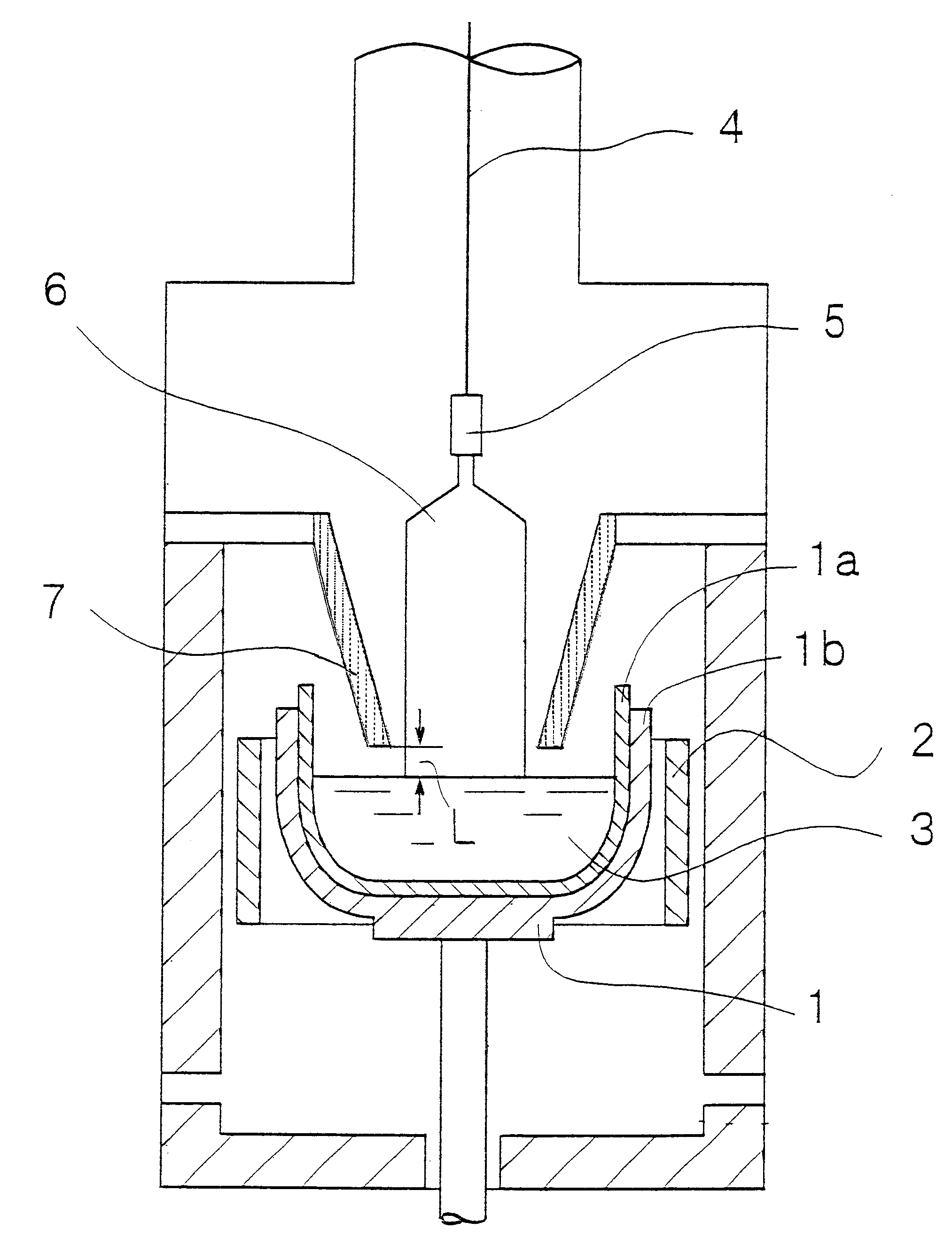
In Example 1, to verify the effects of the second and third manufacturing methods, an 8 inch diameter p-type (100) silicon single crystal was grown using the above-described growing apparatus at a crystal rotating speed of 20 rpm. The single crystal was grown with the nitrogen concentration, oxygen concentration, boron concentration, pull rate, and gap L between the melt surface and the heat shielding material varied. The specific conditions for this growth are shown in Table 1.
Wafers were sliced from the grown single crystal, and the sliced wafers were heat-treated at a high temperature of 1100.degree. C. in an oxygen atmosphere for 16 hours as a heat treatment for OSF density evaluation. The obtained wafer samples were selectively etched for 5 minutes using a Wright etchant, and the OSF density was counted using an optical microscope to determine the location where an OSF ring occurred based on the distance (mm) from the wafer center using the inside diameter of the ring as a refe...
example 2
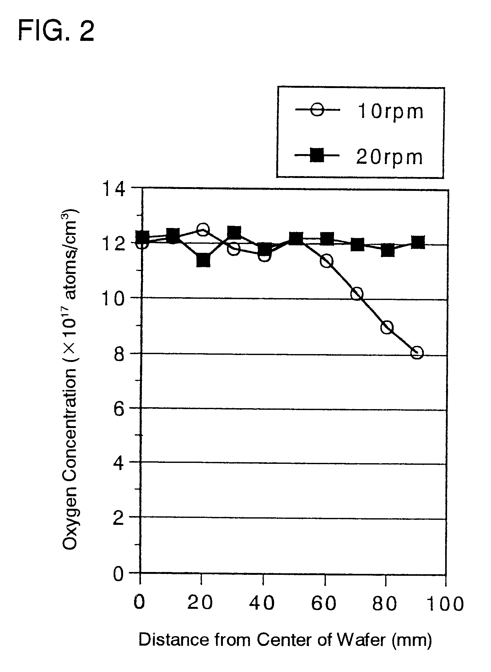
In Example 2, to verify the effect of the first manufacturing method, how in-plane oxygen distributions influence the formation of defects in an epitaxial layer was examined. Two 8 inch diameter p-type (100) single crystals were grown under the condition that each has a nitrogen concentration of 2.times.10.sup.15 atoms / cm.sup.3 and an oxygen concentration of 12.times.10.sup.17 atoms / cm.sup.3. During growth, one of the crystals was rotated at a speed of 20 rpm and the other at a speed of 10 rpm, and the gap L was set to 20 mm for both crystals.
Wafers, which were sliced from the grown crystals, were heat-treated at 1100.degree. C. in an oxygen atmosphere for 16 hours. Samples prepared from the obtained wafers were examined to check oxygen concentration distributions in their in-plane areas through infrared absorption measurement. For oxygen concentration conversion coefficients, the old-ASTM 1979 was used. Then, the samples were selectively etched for 5 minutes using the Wright etchan...
example 3
In Example 3, to verify the effect obtained from the fourth method, techniques were studied for reducing the density of defects in an epitaxial layer by heat-treating a wafer. First, an 8 inch diameter p-type (100) single crystal was grown under the condition that the oxygen concentration is 12.times.10.sup.17 atoms / cm.sup.3, the boron concentration 1.times.10.sup.17 atoms / cm.sup.3, and the crystal rotating speed is 20 rpm while varying the nitrogen concentration within the crystal at two levels, which are 1.times.10.sup.14 atoms / cm.sup.3 and 9.times.10.sup.12 atoms / cm.sup.3.
Each of wafers sliced from the grown crystal was subjected to a pretreatment at various temperatures for various durations before epitaxial layers were grown. After the pretreatment, an epitaxial layer having a thickness of about 5 .mu.m was grown at a deposition temperature of 1150.degree. C. on each wafer. Then, the density of defects in each epitaxial layer was measured using a commercially available surface ...
PUM
| Property | Measurement | Unit |
|---|---|---|
| temperature | aaaaa | aaaaa |
| temperature | aaaaa | aaaaa |
| temperature | aaaaa | aaaaa |
Abstract
Description
Claims
Application Information