Method of forming a quadrupole device for projection lithography by means of charged particles

Inactive Publication Date: 2002-04-02
US PHILIPS CORP
View PDF2 Cites 1 Cited by
  • Summary
  • Abstract
  • Description
  • Claims
  • Application Information

AI Technical Summary

Benefits of technology

It is an object of the invention to make said limitation of the current in the electron beam

Problems solved by technology

Because nowadays in the integrated circuit technique there is a strong tendency to image increasingly larger structures, the throughput during the production of integrated circuits decreases strongly, so that this method of imaging is becoming increasingly more objectionable.
A limit is imposed as regards the curr

Method used


Image

  • Method of forming a quadrupole device for projection lithography by means of charged particles
  • Method of forming a quadrupole device for projection lithography by means of charged particles
  • Method of forming a quadrupole device for projection lithography by means of charged particles

Examples


Embodiment Construction

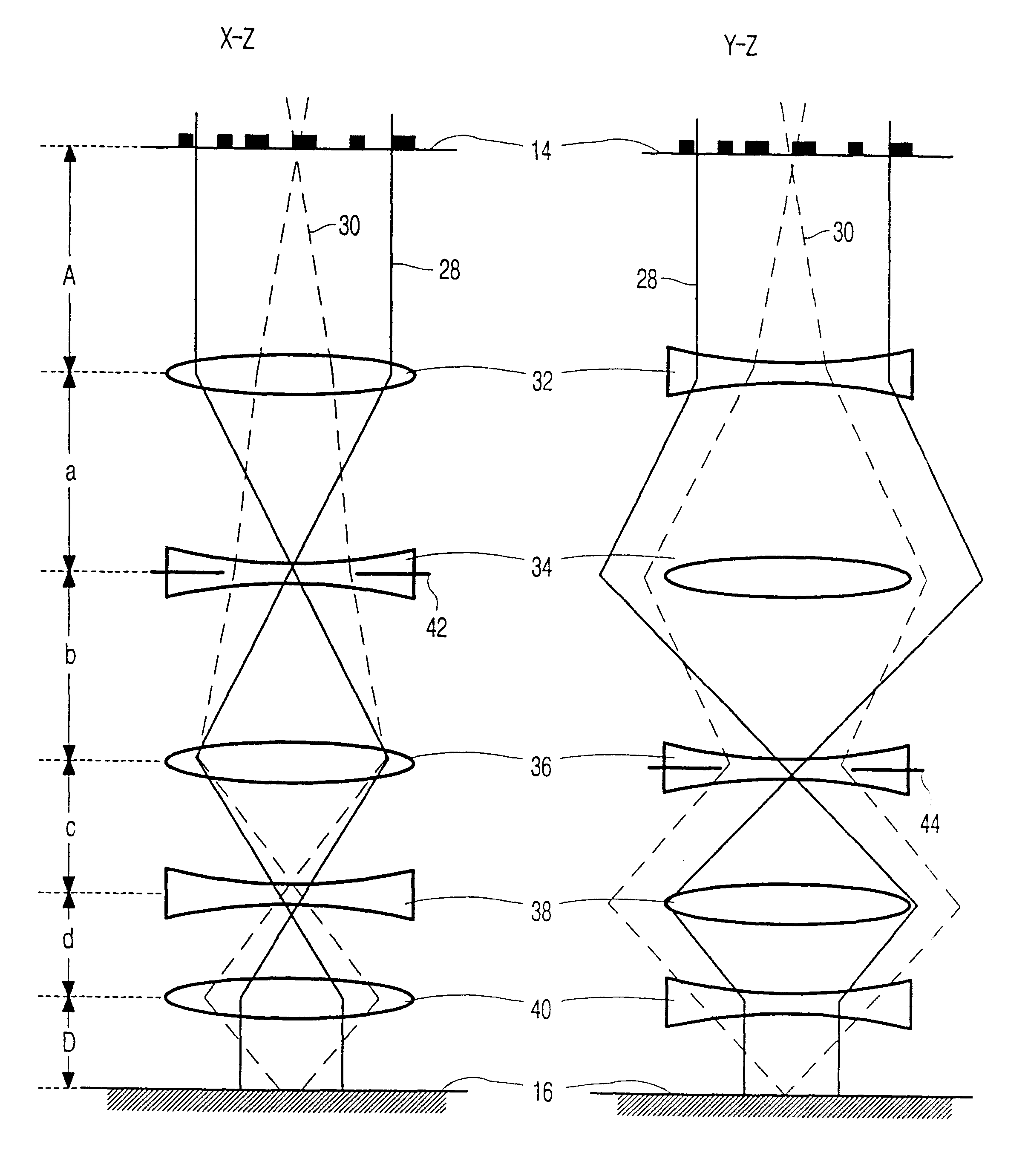
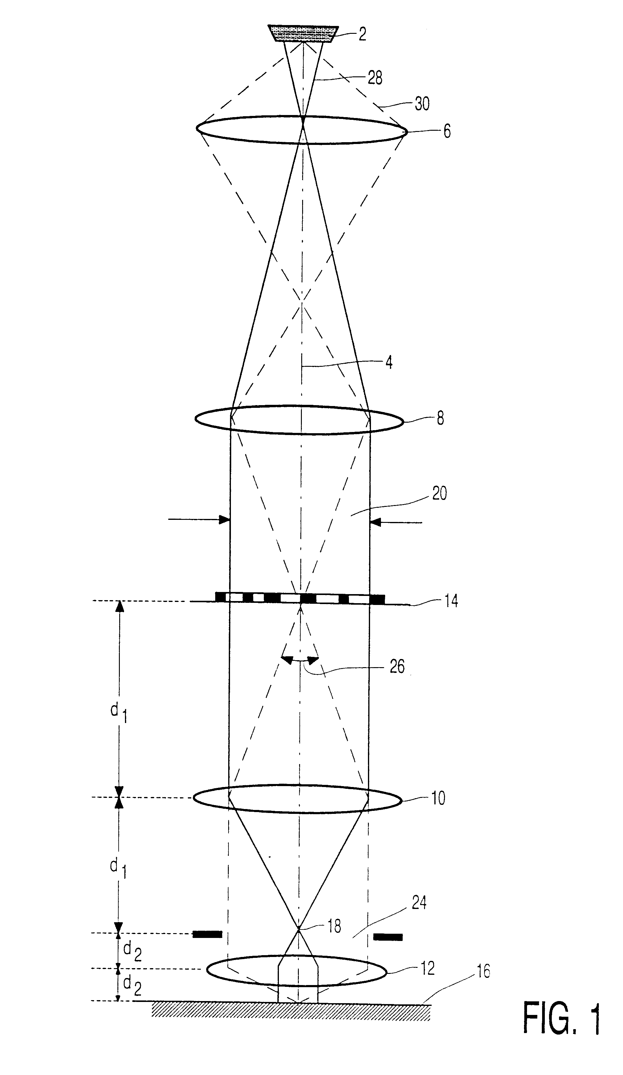
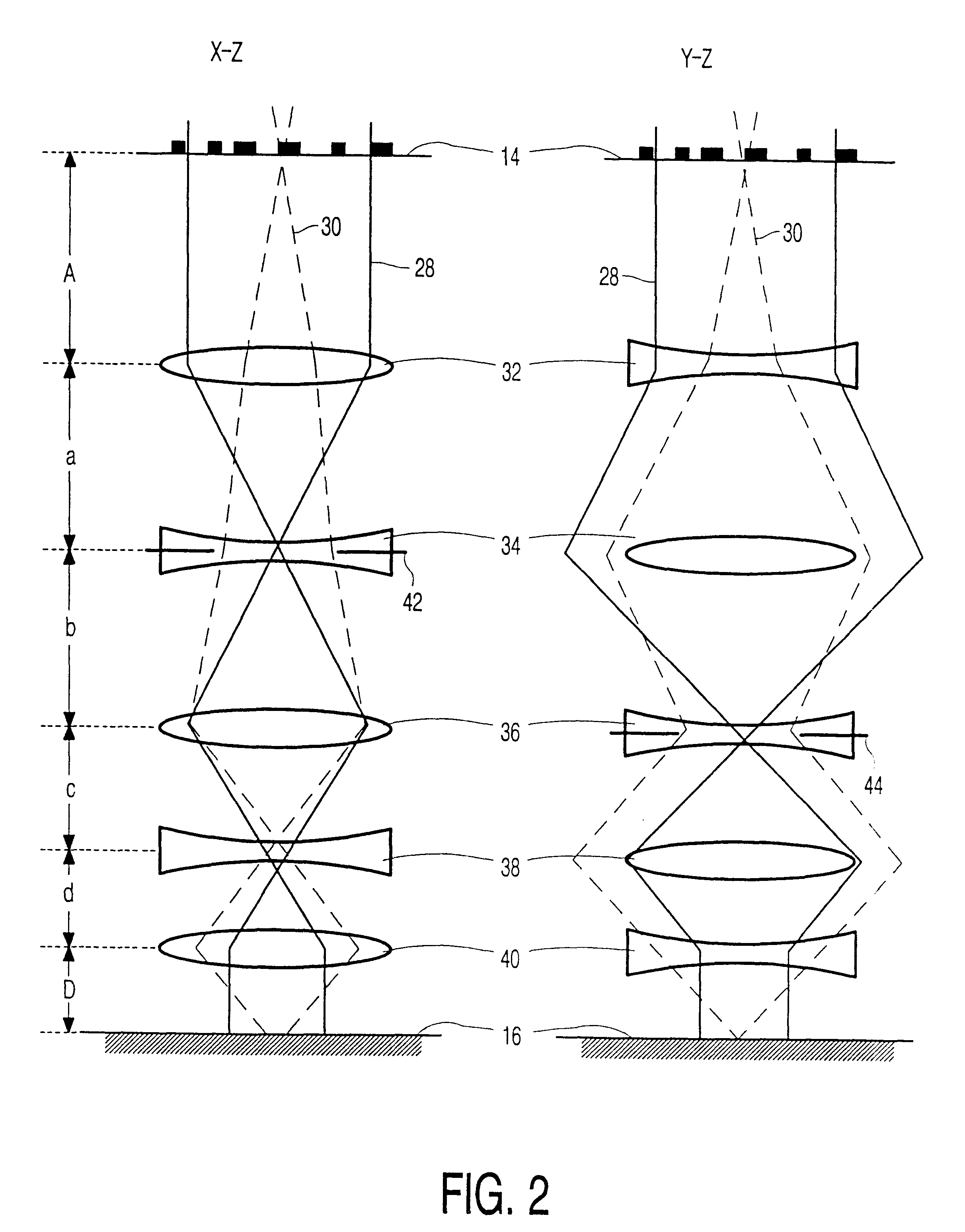
FIG. 1 is a diagrammatic representation of a state of the art imaging particle-optical system for imaging a lithographic object structure on a lithographic imaging surface. In this Figure an electron beam is produced by an electron source 2. The electron beam travels through the lens system along an optical axis 4. The system shown also consists of two round (i.e. rotationally symmetrical) lenses 8 and 10, whose axes coincide with the optical axis of the system. Both lenses 10 and 12 image a lithographic object structure 14 to be imaged, for example a lithographic mask, on a lithographic imaging surface 16, for example a wafer on which integrated circuits are to be formed. In the system shown, the focal length f.sub.1 of the lens 10 equals 160 mm, like the distance d.sub.1 from the mask 14 to the lens 10. The focal length f.sub.2 of the lens 12 equals 40 mm, like the distance d.sub.2 from the lens 12 and the surface of the wafer 16 to be irradiated. It appears from these numbers tha...


PUM


Abstract

According to a known projection lithography method an object is imaged on an imaging surface by means of a telescopic system of rotationally symmetrical electron lenses. The throughput during the production of integrated circuits by means of projection lithography is determined by the amount of current in the imaging electron beam; this current is limited by the resolution-limiting interaction of the electrons (Coulomb interaction). The invention allows for a larger beam current in that areas with a high current concentration are avoided. To this end, the imaging system includes five mutually perpendicular quadrupoles, so that the electrons are concentrated in line-shaped focal spots instead of a (small) circular cross-over. The system is telescopic and the imaging is stigmatic with equal magnifications in the x-z plane and the y-z plane.

Description

The invention relates to a lithography device for carrying out projection lithography by means of charged particles, which device includes an imaging particle-optical system for imaging a lithographic object structure on a lithographic imaging surface.A device of this kind is known from an article in Proceedings SPIE "Electron-Beam Sources and Charged-Particle Optics", Jul. 10-14, 1995, by W. K. Waskiewicz et al., entitled "Electron-Optical Design for the SCALPEL Proof-of-Concept Tool", published in SPIE, Vol. 2522, 1995.Particle-optical imaging, notably electron optical imaging, can be used for the lithographic manufacture of very small structures, such as integrated electronic circuits or masks for such circuits, with a resolution which is less than the wavelength of light.The imaging of a lithographic object structure on a lithographic imaging surface by means of electrons can in principle be carried out in two ways: sequentially and non-sequentially. In the case of sequential im...

Claims


Application Information

Patent Timeline
IPC IPC(8): H01J37/317H01J37/30G03F7/20H01J37/04H01J37/141H01J37/305H01L21/027
CPCB82Y10/00B82Y40/00H01J37/3175H01J37/3007H01J2237/31788H01J2237/04928H01J37/317
Inventor KRIJN, MARCELLINUS P. C. M.
Owner US PHILIPS CORP
Why Eureka
Try Eureka