Method of improving adhesion of capping layers to copper interconnects

a technology of copper interconnects and capping layers, which is applied in the direction of semiconductor devices, semiconductor/solid-state device details, electrical equipment, etc., can solve the problems of poor adhesion of capping layers to cu or cu alloy surfaces, escalating requirements that are difficult to meet, and capping layers such as silicon nitride, deposited by plasma enhanced chemical vapor deposition (pecvd),

Inactive Publication Date: 2002-05-07
ADVANCED MICRO DEVICES INC
View PDF14 Cites 34 Cited by
  • Summary
  • Abstract
  • Description
  • Claims
  • Application Information

AI Technical Summary

Problems solved by technology

Such escalating requirements have been found difficult to satisfy in terms of providing a low RC (resistance capacitance) interconnect pattern, particularly wherein submicron vias, contacts and trenches have high aspect ratios imposed by miniaturization.
There are additional problems attendant upon conventional Cu interconnect methodology employing a diffusion barrier layer (capping layer).
It was found, however, that capping layers, such as silicon nitride, deposited by plasma enhanced chemical vapor deposition (PECVD), exhibit poor adhesion to the Cu or Cu alloy surface.
Consequently, the capping layer is vulnerable to detamination, as by peeling due to scratching, stresses or poor adhesion resulting from subsequent deposition of layers.
As a result, the Cu or Cu alloy is not entirely encapsulated and Cu diffusion occurs, thereby adversely affecting device performance and decreasing the electromigration resistance of the Cu or Cu alloy interconnect member.
Moreover, conventional PECVD silicon nitride capping layers have a density of about 2.62 g / cm.sup.3 and, hence, are not particularly effective as an etch stop layer furring formation of interconnects for subsequent metallization levels.

Method used


Image

  • Method of improving adhesion of capping layers to copper interconnects
  • Method of improving adhesion of capping layers to copper interconnects
  • Method of improving adhesion of capping layers to copper interconnects

Examples


Embodiment Construction

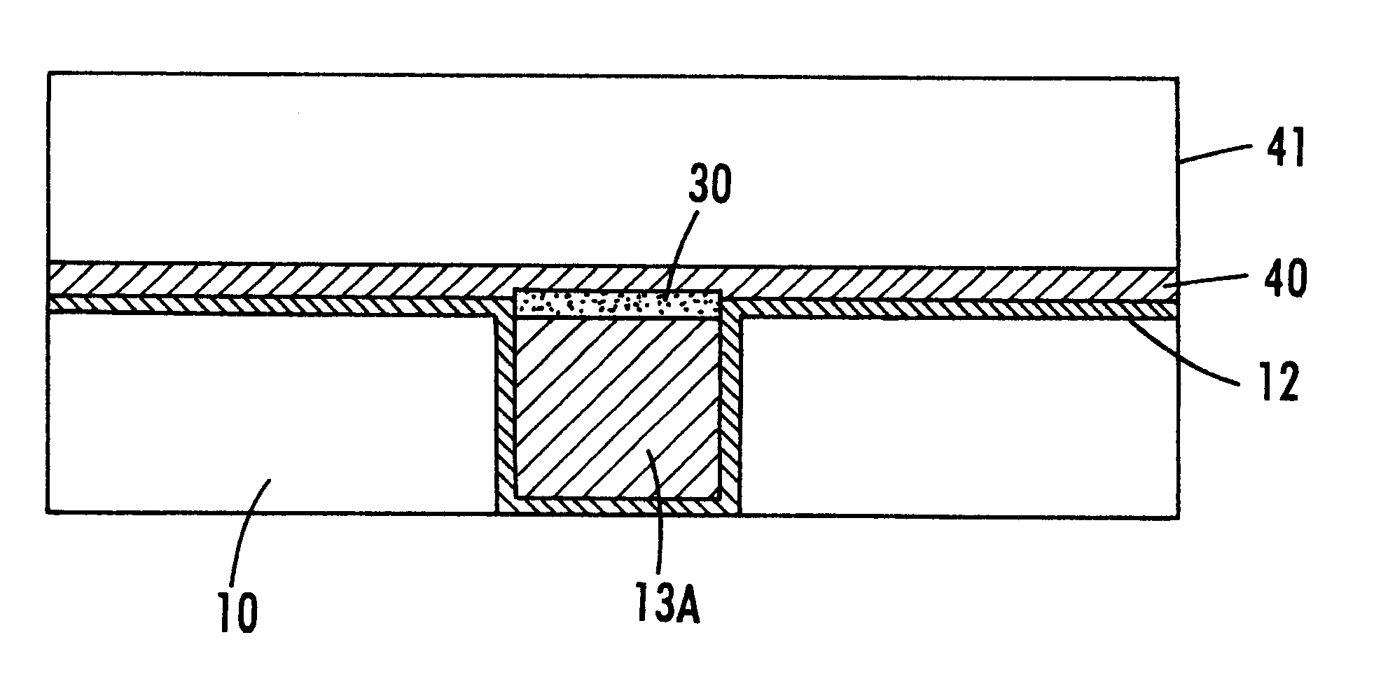
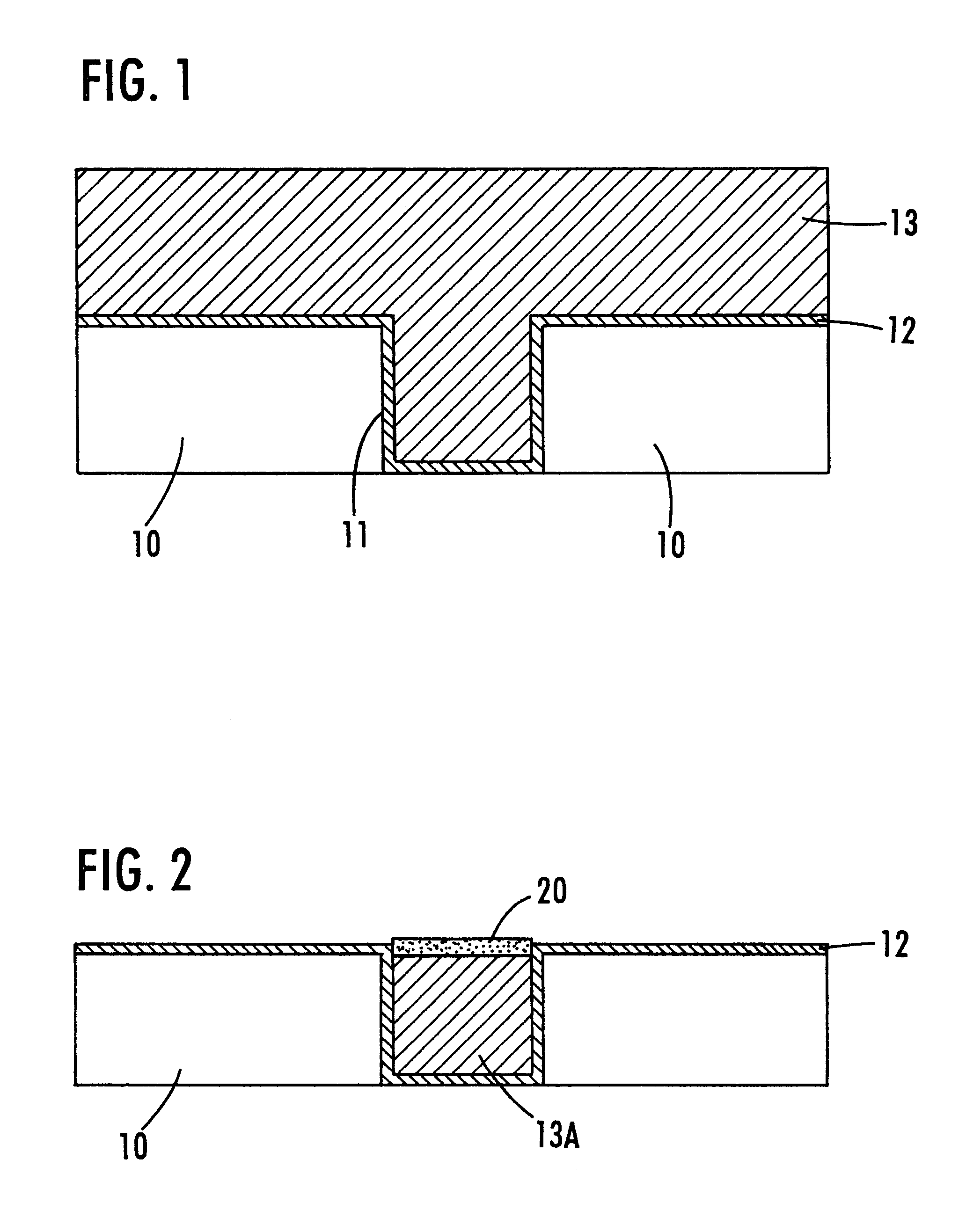
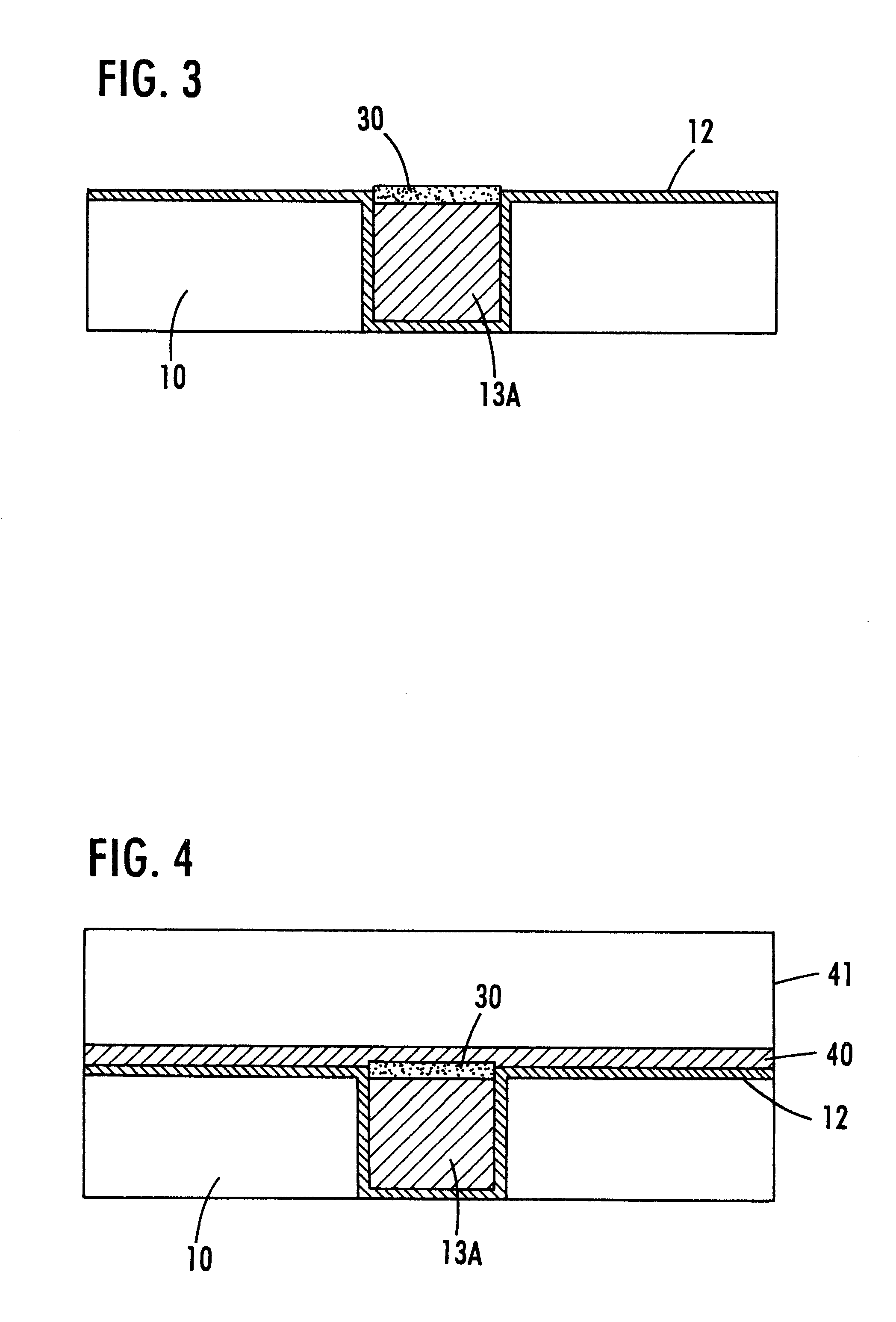
The present invention addresses and solves problems attendant upon capping a Cu or Cu alloy interconnect, as with a capping or barrier layer of silicon nitride. Methodology in accordance with embodiments of the present invention enables a significant improvement in the adhesion of a barrier layer, such as silicon nitride, to a Cu or Cu alloy interconnect member, thereby preventing barrier layer peeling, preventing diffusion and enhancing electromigration resistance. In addition, the present invention provides methodology enabling the deposition of a barrier layer, such as silicon nitride, having a significantly increased density thereby significantly enhancing the ability of the barrier layer to function as an etch stop layer during formation of interconnects for subsequent metallization levels. As employed throughout this application, the symbol Cu is intended to encompass high purity elemental copper as well as Cu-based alloys, such as Cu alloys containing minor amounts of tin, zi...


PUM

PropertyMeasurementUnit
frequency poweraaaaaaaaaa
thicknessaaaaaaaaaa
densityaaaaaaaaaa

Abstract

The adhesion of a barrier or capping layer to a Cu or Cu alloy interconnect member is significantly enhanced by treating the exposed surface of the Cu or Cu alloy interconnect member, after CMP, in a reaction chamber with a plasma containing ammonia and nitrogen for a brief period of time to reduce the surface oxide and then introducing silane into the reaction chamber to deposit the barrier layer, e.g., silicon nitride, under high density plasma conditions in the presence of nitrogen. The presence of nitrogen during plasma oxide layer reduction and plasma barrier layer deposition significantly improves adhesion of the barrier layer to the Cu or Cu alloy surface.

Description

TECHNICALThe present invention relates to copper (Cu) and / or Cu alloy metallization in semiconductor devices. The present invention is applicable to manufacturing high-speed integrated circuits having submicron design features and high conductivity interconnect structures.The escalating requirements for high density and performance associated with ultra large scale integration semiconductor wiring require responsive changes in interconnection technology. Such escalating requirements have been found difficult to satisfy in terms of providing a low RC (resistance capacitance) interconnect pattern, particularly wherein submicron vias, contacts and trenches have high aspect ratios imposed by miniaturization.Conventional semiconductor devices comprise a semiconductor substrate, typically doped monocrystalline silicon, and a plurality of sequentially formed interlayer dielectrics and conductive patterns. An integrated circuit is formed containing a plurality of conductive patterns compris...

Claims


Application Information

Patent Timeline
Patent Type & Authority Patents(United States)
IPC IPC(8): H01L21/70H01L23/532H01L23/52H01L21/768
CPCH01L21/76834H01L23/53238H01L21/76838H01L2924/0002H01L2924/00
Inventor NGO, MINH VANYOU, LUHUERTAS, ROBERT A.ADEM, ERCAN
Owner ADVANCED MICRO DEVICES INC
Why Eureka
Try Eureka