Lateral polysilicon pin diode and method for so fabricating

a polysilicon and pin diode technology, applied in the direction of solid-state devices, electrical devices, semiconductor devices, etc., can solve the problems of insufficient thickness of material and a great deal of charge storage, and achieve the effect of reducing parasitic capacitance and extending the charge storage area

Inactive Publication Date: 2002-07-30
GLOBALFOUNDRIES INC
View PDF6 Cites 15 Cited by
  • Summary
  • Abstract
  • Description
  • Claims
  • Application Information

AI Technical Summary

Benefits of technology

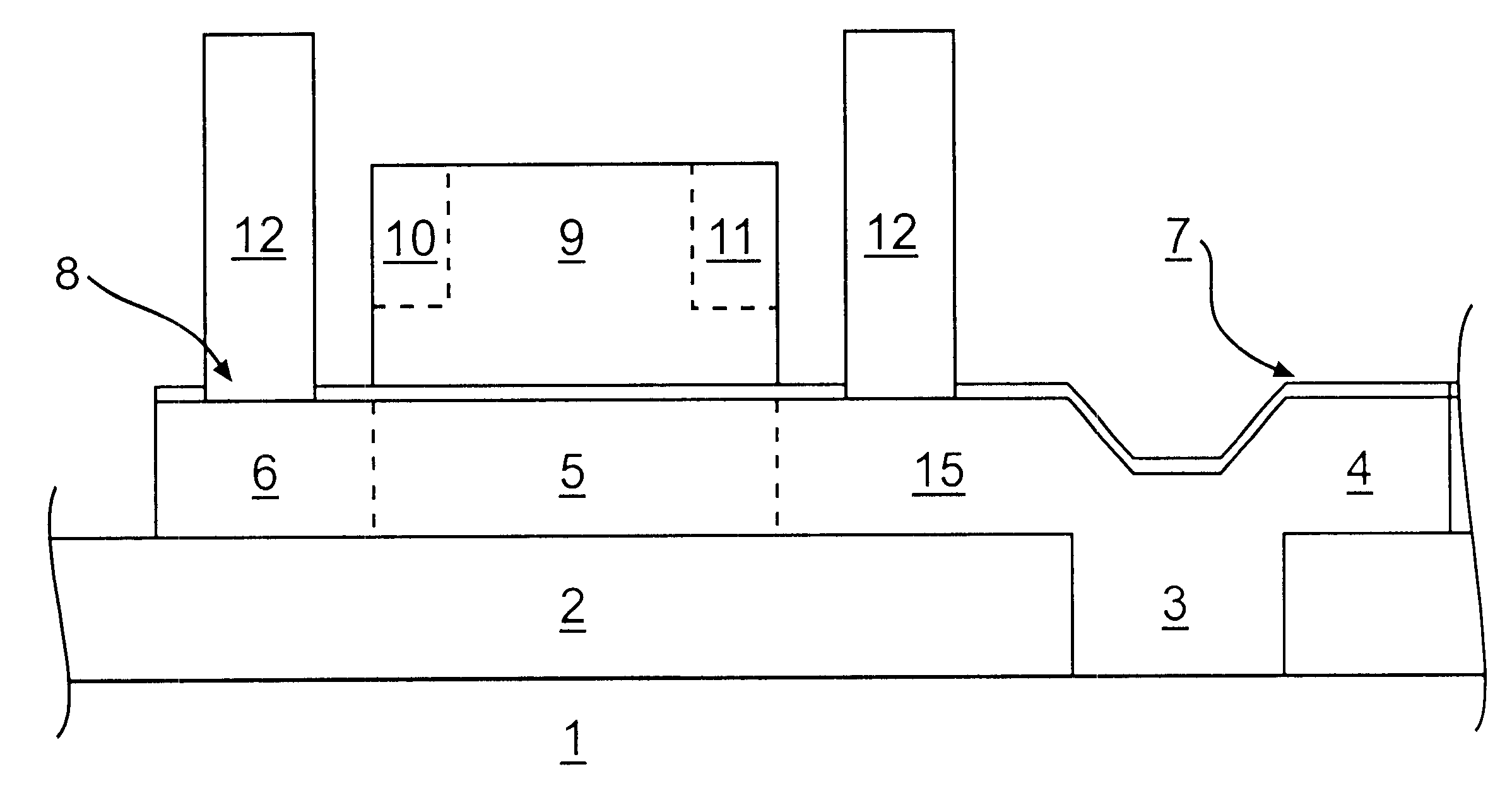
The present invention provides an improved and novel lateral PIN diode structure that laterally extends the intrinsic region thereby extending the charge storage area. The present invention provides for reduced parasitic capacitance by placing the diode on an oxide layer.
The present invention employs polysilicon as the initial material from which the body of PIN is made. Polysilicon doesn't have a great carrier lifetime because carriers can recombine at grain boundaries. This serves to decrease the stored charge, counteracting our attempt to make a large I-layer.
The first embodiment of the invention provides a PIN that can be integrated into an RF chip and which comes for free with the conventional processing steps. This embodiment provides an implant to amorphize the polysilicon and then an anneal step to regrow it as large grain polysilicon to reduce the grain boundaries and improve the carrier lifetime.
In a second embodiment of the invention, the polysilicon comprising the PIN diode layer is caused to pass through an opening in the underlying dielectric layer and to contact the single crystal substrate. The polycrystalline silicon is amorphized and annealed. The surface of the single crystal silicon acts as a seed causing the PIN diode layer to recrystallize as single crystal silicon in a process known as solid phase epitaxy. Thus the I-layer of the PIN diode will be caused to have high carrier lifetimes.

Problems solved by technology

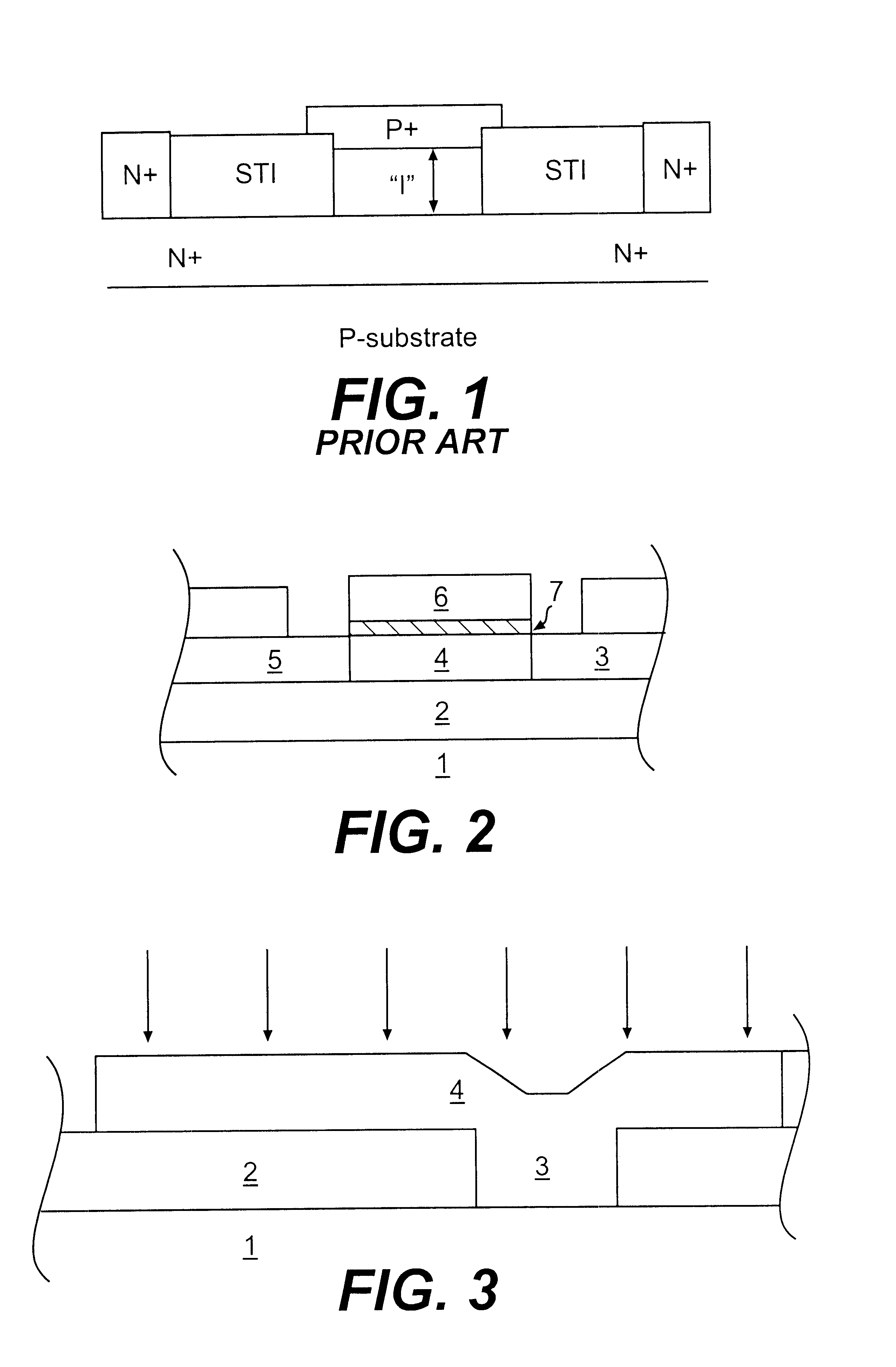
In addition, a great deal of charge gets stored in the "I" region of the device.
There simply isn't enough thickness of material to make a large I region in a PIN diode by growing the I-layer in the vertical direction.

Method used


Image

  • Lateral polysilicon pin diode and method for so fabricating
  • Lateral polysilicon pin diode and method for so fabricating
  • Lateral polysilicon pin diode and method for so fabricating

Examples


first embodiment

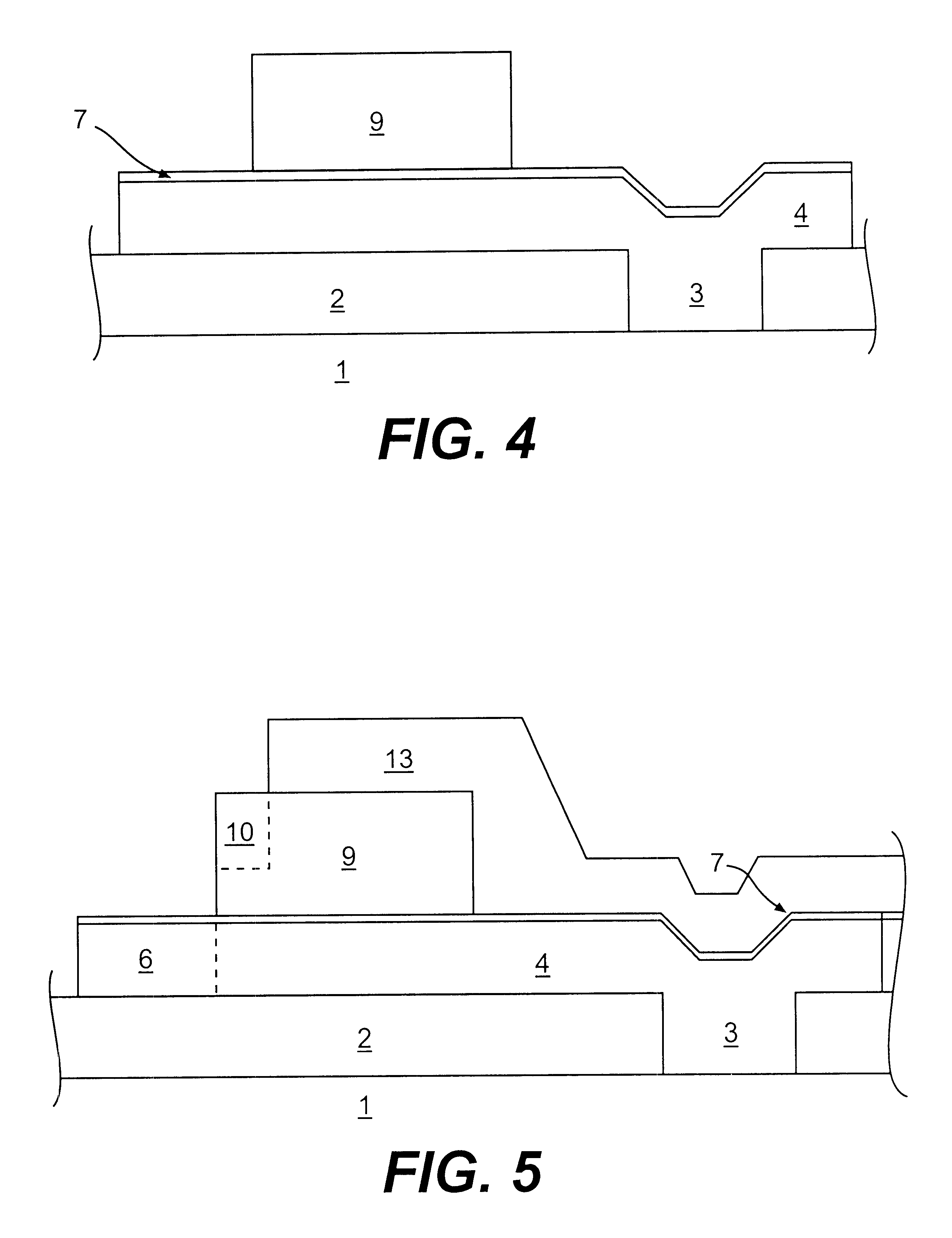
Referring now to FIG. 2. The first version comes for free in an epitaxial-base bipolar process such as silicon-germanium BICMOS technology. The semiconductor substrate 1 is standard as is the about 2800 .ANG. oxide layer 2 provided on a top surface. The base polysilicon is used to form the body of the PIN diode and is appropriately masked and doped to yield N+3, intrinsic (I) 4, and P+5 regions. Emitter-base passivation 7 is used to form the passivating layer for the polysilicon, to help reduce the surface recombination by using a high-quality thermal oxide interface. The emitter polysilicon 6 forms a masking layer that prevents future implants from getting into the body of the diode. On this polysilicon layer, the edges of the masks for P+ and N+ implants on either side of the PIN diode body are defined. Prior art PIN diodes are restricted to I-regions of about 0.5 .ANG. by the thickness of the epitaxial layer in which it is formed. By arranging the I-region laterally, the present ...

second embodiment

In an alternative embodiment, an extra mask can be used to open a region of the base polysilicon over the single crystal base, through the emitter-base passivation. The amorphous silicon layer used for the passivation can then be deposited and annealed. This results in epitaxial lateral growth of the amorphous silicon from the seed area in the single crystal base. This results in a single crystal structure which has reduced recombination current. In a fashion similar to the first embodiment, a passivation and masking layer can be formed on top, and the P+ and N+ implants can be defined into opposite ends of the diode body.

Turning now to FIG. 3, a sequence of steps for fabrication of a second embodiment is recited. This recitation refers to a preferred embodiment wherein the substrate is silicon. Therefore, silicon-specific means, such as silicon-specific isolations and process steps are recited. However, it is to be understood that the present invention is capable of being realized ...


PUM


Abstract

The invention provides a PIN diode having a laterally extended I-region. The invention also provides a method of fabricating the inventive PIN diode compatible with modern RF technologies such as silicon-germanium BiCMOS processes.

Description

The present invention relates to PIN diodes and particularly a diode structure wherein the various conductive regions are laterally disposed.Electronic switches are key for a large variety of applications, in particular, the very high volume consumer wireless 1-2 GHz market where they serve to switch the antenna in a mobile phone between receive and transmit circuits. A good switch must possess several important properties. First, the resistance should be low when the switch is on. Second, the isolation should be good when the switch is off. Finally, the switch should be able to handle a signal of sufficient strength without distorting it (i.e. without the signal itself causing the switch to turn further on or off compared to its initial state).One type of switch has been very successful at high frequencies is the PIN diode, which consists of an intrinsic or "I" region sandwiched between P and N regions. When this diode is reverse biased (P region at a negative voltage compared with...

Claims


Application Information

Patent Timeline
Patent Type & Authority Patents(United States)
IPC IPC(8): H01L29/66H01L29/868
CPCH01L29/868Y02E10/548
Inventor GREENBERG, DAVID R.JADUS, DALE K.SUBBANNA, SESHADRIWALTER, KEITH M.
Owner GLOBALFOUNDRIES INC
Why Eureka
Try Eureka