Optoelectronic connector system

Inactive Publication Date: 2002-08-13
ALTERA CORP
View PDF11 Cites 28 Cited by
  • Summary
  • Abstract
  • Description
  • Claims
  • Application Information

AI Technical Summary

Problems solved by technology

This issue holds true for data transfer within an integrated circuit, from one chip to another, from hybrid circuit to hybrid circuit, from one integrated circuit board to another integrated circuit board, and from system to system.
Under such an approach, there is always a greater processing capability available on a chip than off it, and so, unfortunately, advances in chip design must wait for the rest of the system to catch up.
Accelerated development of wider bit buses (e.g. 128, 256, etc.) has been impeded by several factors including the practical limitation on the size of the mechanical connectors, the noise inherent in the signals arriving nearly simultaneously, the reliability of wide pin connectors, and the power required to drive multiple lines off-chip.
Increasing the processor speed is not without challenges, however, because increasing the speed also increases power requirements, introduces skew problems across the channel, and usually requires more exotic proces

Method used


Image

  • Optoelectronic connector system
  • Optoelectronic connector system
  • Optoelectronic connector system

Examples


Example

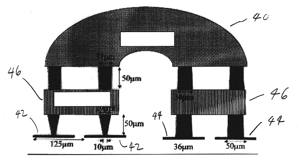
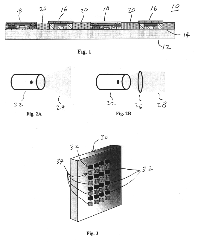
As shown in FIG. 1, an optoelectronic device 10 is provided, consisting of a silicon substrate 12. On the upper surface of substrate 12, alternating detectors 16 and laser emitters 18 are attached with epoxy filler 20 therebetween. Each emitter has a means for electrical connectivity embedded in the chip and connected to the chip substrate and package. Typical emitters may be 10 .mu.m in size, constructed on 125 .mu.m centers. Similarly, a detector array is constructed using detectors 50 .mu.m in size, spaced identically to the emitter array. In FIG. 3, an array of emitters 32 and detectors 34 are attached to substrate 30.

One problem with optical emitters is that the light produced is uncollimated, that is, it will disperse over some angle, as shown in FIG. 2A where emitter 22 produces uncollimated light 24. As shown in FIG. 2B lens 26 can be used to produce collimated light 28. This is useful for transmission both through free space through fiber optic media.

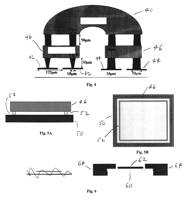
As shown in FIG. 4, the...


PUM


Abstract

An optical transceiver system including a plurality of transceiver nodes with at least one two-dimensional integrated circuit array of optical emitters and detectors mounted on an ASIC drive circuit and forming a focal plane; a lens or light collimator located adjacent for directing light to and from the emitter and detectors; an epoxy stand off located peripherally around each focal plane to prevent contact between the focal plane and the lens or collimator and to prevent entry of contaminants therebetween; and at least one fiber optic bundle to convey light between each of the transceiver nodes through the perspective lenses or collimators.

Description

This invention relates to optical communication systems and more particularly to a fiber optic cable and transceiver connector system utilizing a coherent bundle of optical fibers, or image guide, or ordered fiber array.BACKGROUND OF INVENTIONOptical couplers are now used to communicate optical signals over short and long distances between, for example, two computers, two circuit boards in one computer, and even two different chips on the same circuit board. Communications of this type are also disclosed in a co-pending patent application filed on even date herewith, entitled "Optical Communication Network with Receiver Reserved Channel", Timothy P. Boggess and John A. Trezza, incorporated herein by reference.The technology associated with electronics has evolved extremely rapidly over the last 40 years. Computers and related peripheral equipment, satellite, and communication systems are becoming ever more sophisticated and powerful. A key factor leading to every increasing demand f...

Claims


Application Information

Patent Timeline
IPC IPC(8): G02B6/42G02B6/43H04B10/207H04B10/12H04B10/272
CPCG02B6/4249G02B6/4292G02B6/43H04B10/40G02B6/4246H01L2221/68359
Inventor TREZZA, JOHN A.
Owner ALTERA CORP
Why Eureka
Try Eureka