Method of forming MOS transistor

a transistor and mos technology, applied in the field of forming mos transistors, can solve problems such as harmful effects, variable problems, and transistors that do not perform normal operations

Inactive Publication Date: 2002-08-20
RENESAS ELECTRONICS CORP
View PDF3 Cites 37 Cited by
  • Summary
  • Abstract
  • Description
  • Claims
  • Application Information

AI Technical Summary

Problems solved by technology

Notwithstanding, if the device is scaled down and a further high performance is required, then this is the important technical issue.
The introduction of the large amount of fluorine ions, however, causes many inter-lattice silicon atoms introduced into the substrate upon fluorine implantation.
But as the transistor is scaled down and for example, the gate length is not more than 0.15 micrometers, then the variation is problem.
If, however, the impurity concentration of the channel region is simply lowered, a punch-through phenomenon appears whereby it is possible that the transistor does not perform the normal operations.
Accordingly, if the problem with the slow trap can be solved, then a new harmful effect of reducing the stability in performance of the integrated circuit is caused.
Only changing the timing of the fluorine introduction is difficult for preventing the enhanced diffusion.
This method, however, provides a damage to the gate oxide film in the ion-implantation.
Particularly, in the scaled down transistor, the thickness of the gate oxide film is thin and the damage by the ion-implantation is large, whereby the above problem is remarkable.
The slow trap problem is not considered and no solution is proposed.
As a result, the impurity profile of the channel region is changed to cause variation in Vth (boron punch-through problem).
On the channel region of the interface of between the gate insulating film and silicon of the substrate, large amounts of dangling bonds of silicon and Si--H bonds reside, for which reason the problem with the slow trap can not be solved.
On the interface between the gate insulating film and silicon of the substrate, large amounts of dangling bonds of silicon and Si--H bonds reside, whereby the slow trap problem can not be solved.
Fluorine introduced in the gate oxide film causes the problem with the boron punch-through problem.
In accordance with this technique, if the refractory metal silicide layer is formed over the above regions, then the shape of the silicide surface is deteriorated and the increase in the resistance of the silicide layer is caused.
In this case, the remarkable reductions in the performance and the yield of the transistor are caused.
Particularly in the scaled down device, for example, the transistor having the gate electrode of a gate length of not more than 0.15 micrometers, the variation in threshold voltage is problem.
Even the fluorine ions are implanted into the gate electrode, the problem with the boron punch-through is unlikely to be caused even the fluorine ions into the gate electrode.
If the first and second heat treatments are concurrently carried out, the above problem is also raised.
If the temperature is too low, then the substitution of fluorine is insufficient, and the effect of the improvement to the slow trap characteristic is insufficient.
As a result, the formed cobalt silicide film is inferior in etching resistivity and is likely to be eluted into an etching solution in the process for removing the unrea...

Method used


Image

  • Method of forming MOS transistor
  • Method of forming MOS transistor
  • Method of forming MOS transistor

Examples


embodiment 1

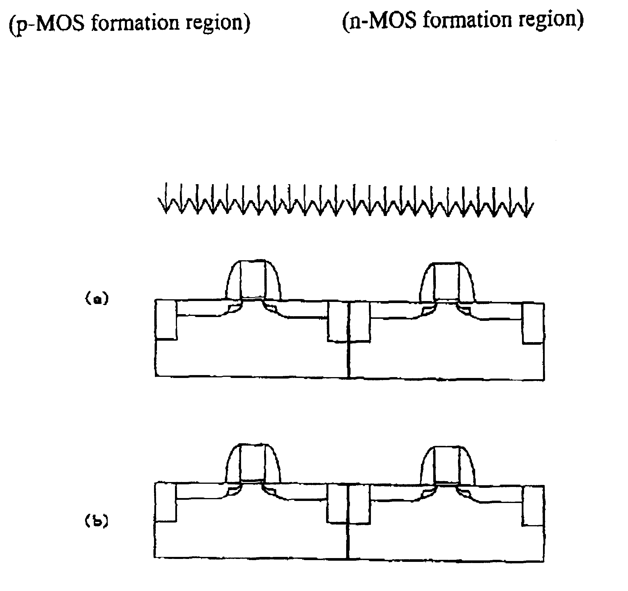
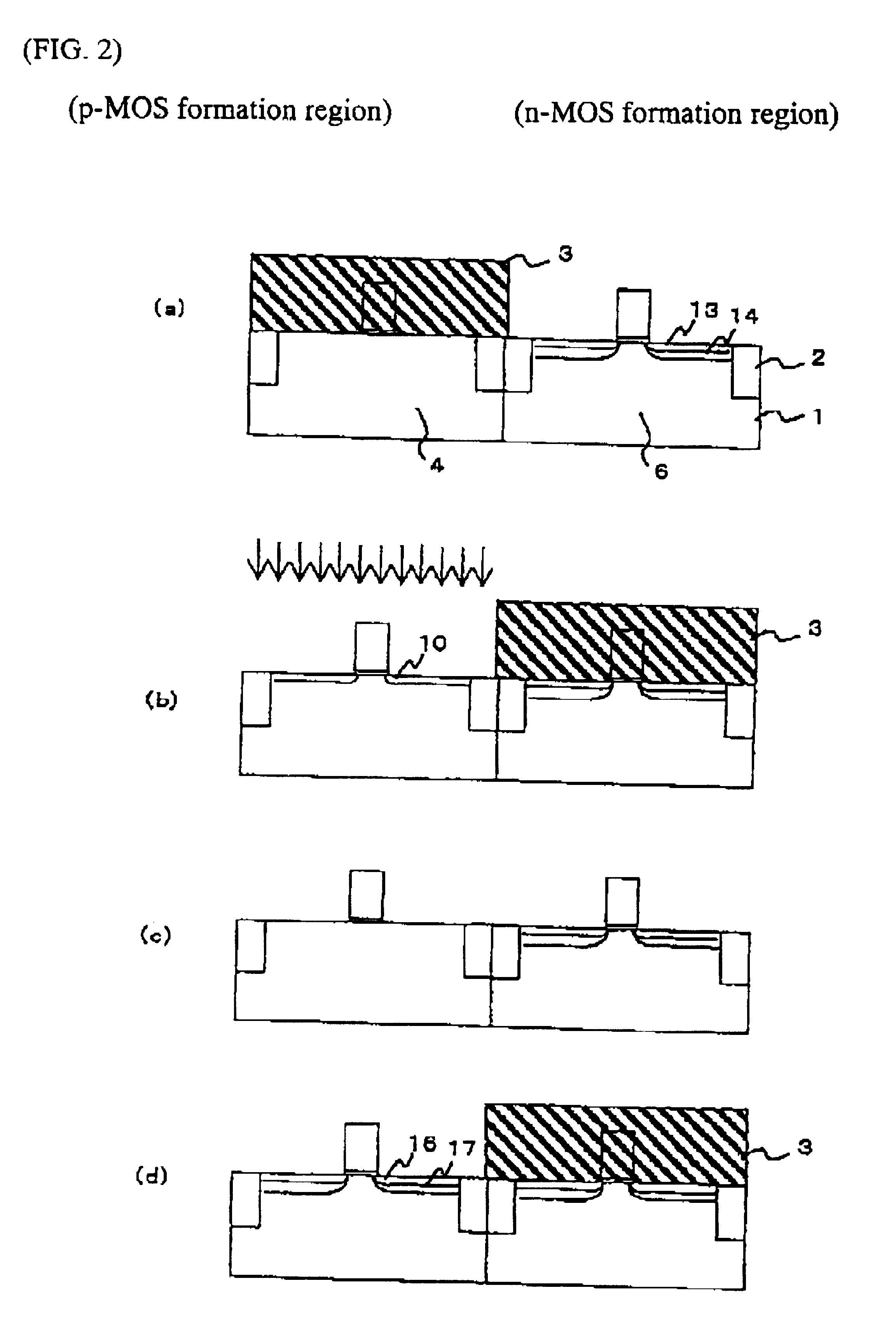
The present embodiment is to apply the present invention to the CMOS fabrication processes. The description will be made with reference to FIGS. 1-4. The heat treatment temperature mentioned below is the temperature hen measuring the substrate temperature by a non-contact measurement for example pyrometer.

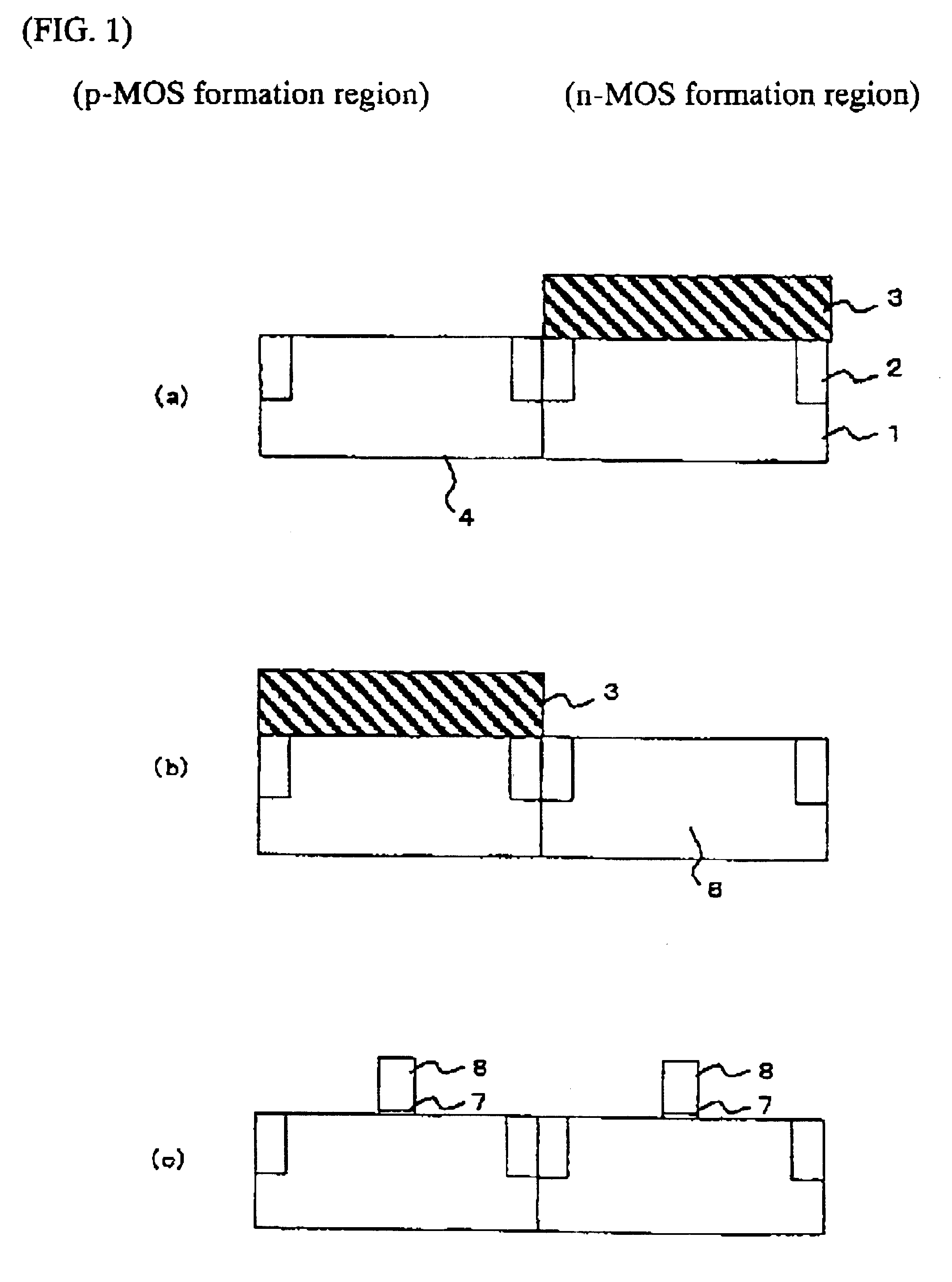
As shown in FIG. 1(a), a shallow trench isolation 2 is formed over a silicon substrate 1. A photo-resist 3 is provided on an n-MOS formation region for carrying out an ion-implantation of phosphorus into a p-MOS formation region, thereby forming an n-well 4. The photo-resist 3 remains and an ion-implantation of As is carried out for adjusting a threshold voltage. The conditions for the ion-implantation is that the acceleration voltage is 100 keV and the dose is 6.times.10.sup.12 cm.sup.-2.

As shown in FIG. 1(b), a photo-resist 3 is provided on the p-MOS formation region for carrying out an ion-implantation of boron into the n-MOS formation region to form a p-well region 6. The photo...

embodiment 2

This embodiment is to show an example for applying the present invention to the CMOS fabrication process through the similar processes to the example 1. In example 1, the ion-implantation of fluorine for improvement in the slow trap is carried out to only the p-MOS formation region at the acceleration voltage of 15 keV and the dose of 1.times.10.sup.14 m.sup.-2. In this embodiment, immediately after the gate patterning process FIG. 1(c), the ion-implantation of fluorine is carried out under the acceleration voltage of 15 keV and the dose of 3.times.10.sup.15 m.sub.-2. In example 1, the ion-implantation of arsenic for forming the source and drain of the n-MOS (FIG. 3(c)) is carried out at the acceleration voltage of 30 keV and the dose of 6.times.10.sup.15 m.sup.-2. In this embodiment, the ion-implantation of fluorine is carried out under the acceleration voltage of 50 keV and the dose of 1.times.10.sup.15 m.sup.-2.

example 3

This embodiment is to show an example for applying the present invention to the CMOS fabrication process through the similar processes to the example 1. In example 1, the ion-implantation of fluorine for improvement in the slow trap is carried out to only the p-MOS formation region at the acceleration voltage of 15 keV and the dose of 1.times.10.sup.14 m.sup.-2. In this embodiment, immediately after the gate patterning process FIG. 1(c), the ion-implantation of fluorine is carried out under the acceleration voltage of 15 keV and the dose of 3.times.10.sup.15 m.sup.-2.


PUM


Abstract

(issue) It is an issue to suppress variation in threshold voltage due to deterioration in shot channel characteristics and improve the slow trap characteristics of the MOS transistor for suppressing variation in threshold voltage of the transistor for a long-term use.(means for solving the issue) fluorine ions are implanted into a surface of a silicon substrate 1 but a peripheral region of a gate electrode on a p-MOS formation region. A first heat treatment is carried out for removing inter-lattice silicon atoms generated upon ion-implantation. Thereafter, a second heat treatment is carried out for diffusing fluorine ions into a region directly under the gate electrode. The first heat treatment is a lamp anneal such as RTA, and the second heat treatment is a furnace anneal.

Description

The present invention relates to a technique for improving a variation in threshold voltage of an MOS transistor through a long term use.PRIOR ARTThe conventional fabrication method for the MOS transistor will be explained with reference to FIGS. 17-19 by taking an example of CMOS (complementary MOS transistor) fabrication processes.As shown in FIG. 17(a), after an isolation film 2 is formed on a silicon substrate 1, a photo-resist 3 is provided on an n-MOS formation region so that an n-type impurity such as phosphorus is ion-implanted into a p-MOS formation region, whereby an n-type well 4 is formed. Subsequently, the photo-resist 3 remains and an impurity is ion-implanted for adjustment to a threshold voltage. Subsequently, as shown in FIG. 17(b), a photo-resist 3 is provided on the p-MOS formation region for ion-implantation of a p-type impurity into the n-MOS formation region, whereby a p-type well 6 is formed. Subsequently, the photo-resist 3 remains and an impurity is ion-impl...

Claims


Application Information

Patent Timeline
IPC IPC(8): H01L21/02H01L21/265H01L21/8238H01L21/324H01L21/70H01L21/28H01L21/336H01L27/092H01L29/78
CPCH01L21/26506H01L21/324H01L21/823807H01L21/823814H01L21/2658
Inventor ONO, ATSUKIHAMANAKA, NOBUAKI
Owner RENESAS ELECTRONICS CORP
Why Eureka
Try Eureka