

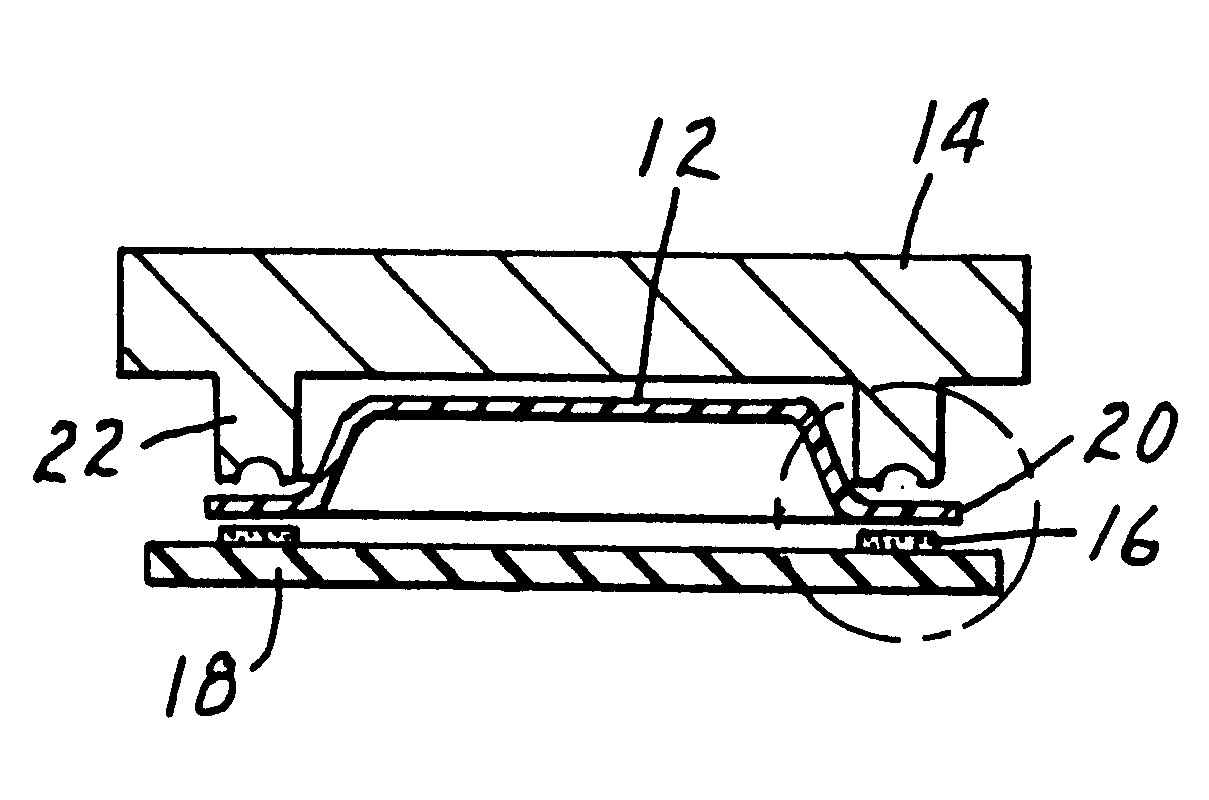
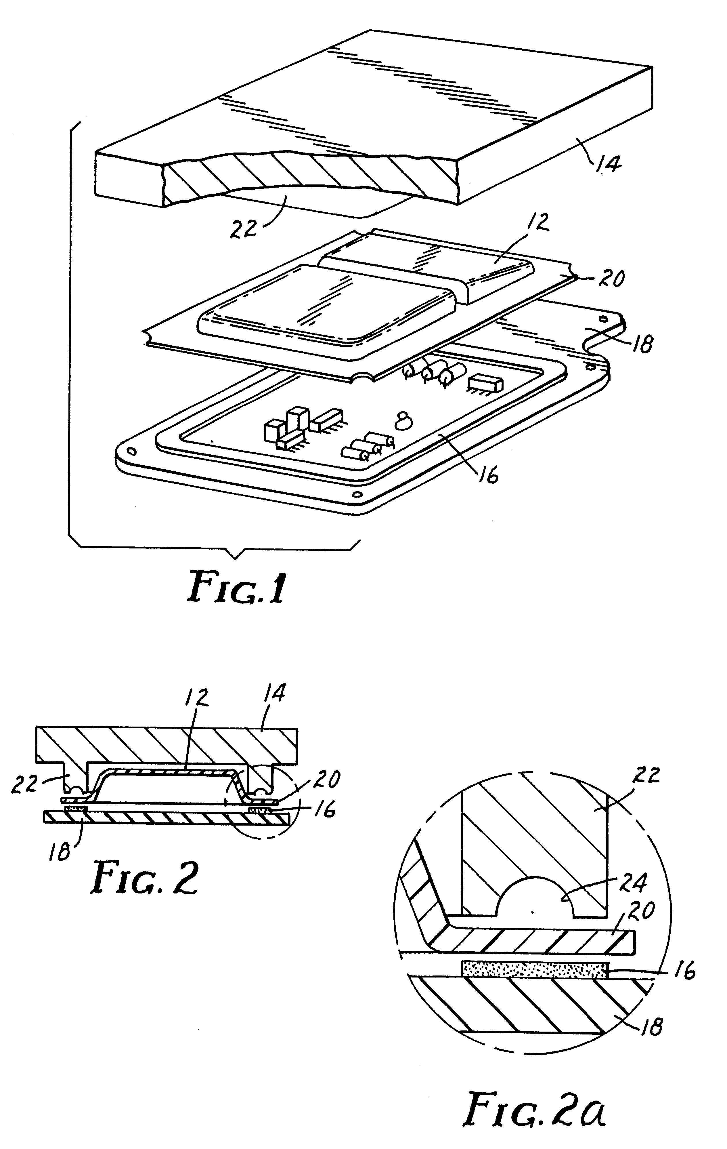
EMI shielding enclosures
a shielding material and shielding technology, applied in the field of electronic assemblies, can solve the problems of affecting the shielding effect of metal layers,
- Summary
- Abstract
- Description
- Claims
- Application Information
AI Technical Summary
Benefits of technology
Problems solved by technology
Method used
Image

Examples
example 2c
Fiber mat A was formed directly on one surface of a sheet of 0.25 mm thick polycarbonate (GE #8B35 V / M--from GE Plastics-Structured Products). A film of 0.15 mm thick ethylene vinyl acetate (BYNEL E 418--available from E.I. DuPont de Nemours), extruded at 235.degree. C. over the metal fibers, provided a sandwich composite which then passed through a pair of heated nip rollers. The chromed steel roller, next to the BYNEL E 418 layer, operated at a surface temperature of 113.degree. C. with a silicone release liner interposed to prevent sticking of the layer to the roller surface. A rubber roller, controlled at 96.degree. C. abutted the surface of the polycarbonate sheet. At the prevailing temperatures of the rollers, there was insufficient polymer flow to substantially surround the metal fibers. The appearance of the laminate provided evidence of air entrapment between the layers of film and the fiber mat. A thermoformed sample, of the sandwich composite, revealed evidence of bleedin...
example 3
Fiber mat A was formed directly on a surface of a sheet of 0.25 mm thick polycarbonate (LEXAN 8010MC from GE Plastics-Structured Products). A 0.20 mm thick film of ethylene vinyl acetate (BYNEL E 418 available from E.I. DuPont de Nemours), extruded at 235.degree. C. over the top of the metal fibers, sealed them between polymer layers. The resulting composite then passed through a gap of about 0.50 mm formed by nip rollers operating at 121.degree. C. A silicone release cover, over the roller contacting the BYNEL side of the composite, prevented sticking at the interface.
example 4
A sheet of 0.25 mm thick polycarbonate (LEXAN 8010MC from GE Plastics-Structured Products) was coated with ethylene vinyl acetate (BYNEL E 418 available from E.I. DuPont de Nemours) to a thickness of 0.10 mm, using extrusion coating at 235.degree. C. The next step of composite preparation involved formation of metal fiber mat A against the layer of ethylene vinyl acetate. A 0.10 mm thick film of ethylene vinyl acetate (BYNEL E 418 available from E.I. DuPont de Nemours), extruded at 235.degree. C. over the top of the metal fibers, then sealed them between layers of ethylene vinyl acetate. The resulting composite then passed through a gap of about 0.50 mm between a steel roller and a back-up rubber roller, forming nip rollers, operating at 113.degree. C. A silicone release cover, over the steel roller contacting the BYNEL side of the composite, prevented sticking at the interface.
PUM
 Abstract
Description
Claims
Application Information