Metal mask etching of silicon

a metal mask and etching technology, applied in the direction of vacuum evaporation coating, transistors, coatings, etc., can solve the problems of insufficient micromachining applications, insufficient deep trench capacitor fabrication, insufficient deep trench isolation, etc., and the sidewall profile of the trench is difficult to control

Inactive Publication Date: 2002-12-10
APPLIED MATERIALS INC
View PDF11 Cites 42 Cited by
  • Summary
  • Abstract
  • Description
  • Claims
  • Application Information

AI Technical Summary

Problems solved by technology

While 40:1 selectivity is acceptable for a number of fabrication applications, such as gate type field effect transistors, it is not adequate for many micromachining applications, or for fabrication of deep trench capacitors, deep trench isolation (DTI) for high frequency circuitry, power devices, and numerous other applications.
For example, with respect to especially deep trenches of the kind required for deep trench capacitors used in DRAM cells where the trench may be 200 .mu.m deep, a 40:1 selectivity would require a silicon oxide mask thickness of about 5 .mu.m, which causes numerous problems.
Use of such a thick masking layer of silicon oxide makes it more difficult to control the sidewall profile of the trench as it is etched; since, as etching pr

Method used


Image

  • Metal mask etching of silicon
  • Metal mask etching of silicon
  • Metal mask etching of silicon

Examples


example two

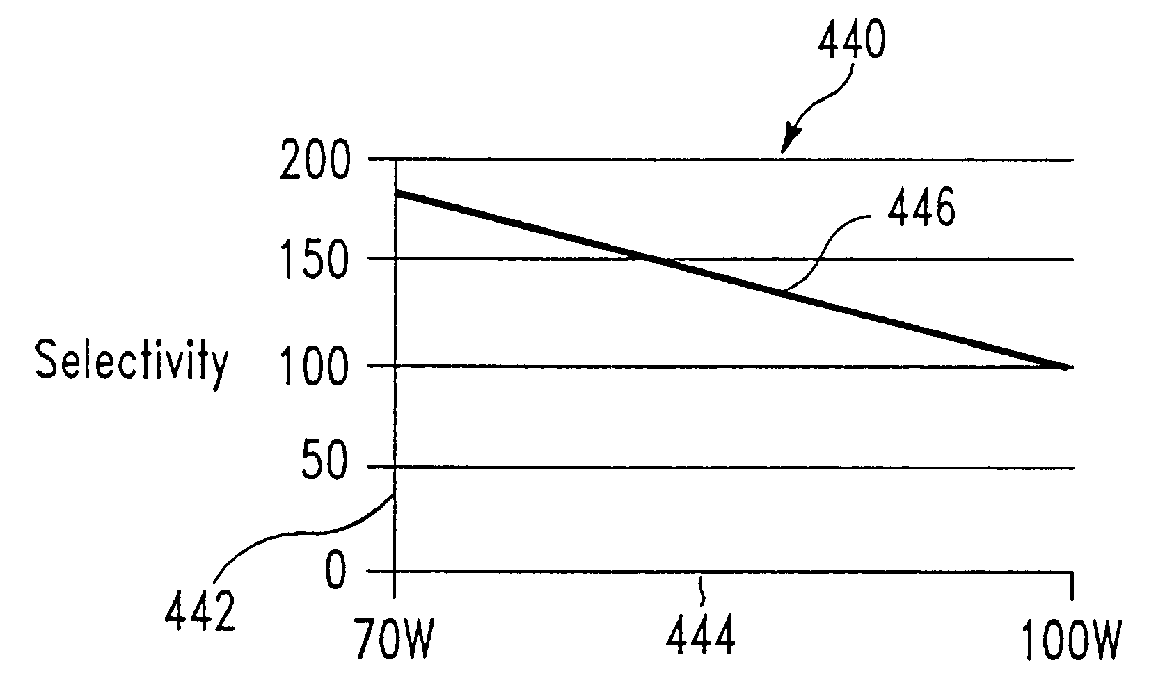
In this Example, 5 experiments were conducted. The film substrate etched was similar to that described with reference to EXAMPLE ONE in terms of the width of the lines and spaces between the lines. However, the line structure was different, as is illustrated in FIG. 4A. The film structure 400 included a line 401 resting on the upper surface 403 of single crystal silicon substrate 402. Line 401 had an overall thickness 404 of 5.34 .mu.m, including: a 4,000 .ANG. thick layer of TEOS 404 in direct contact with upper surface 403; a 1,400 .ANG. thick layer of Si.sub.3 N.sub.4 406 overlying the TEOS layer 404; a 40,000 .ANG. (4.0 .mu.m) thick masking layer 408 of Al--Cu overlying the Si.sub.3 N.sub.4 layer 406; and a second, 8,000 .ANG. thick TEOS layer 410 overlying the Al--Cu masking layer 408.

A pre-clean plasma etch step is optional prior to the etch step described in Table II below. When it is used, it is for purposes of removing debris (such as native oxide) from the portion of the s...


PUM

PropertyMeasurementUnit
Percent by massaaaaaaaaaa
Pressureaaaaaaaaaa

Abstract

The present disclosure provides a method for etching trenches, contact vias, or similar features to a depth of 100 mum and greater while permitting control of the etch profile (the shape of the sidewalls surrounding the etched opening). The method requires the use of a metal-comprising masking material in combination with a fluorine-comprising plasma etchant. The byproduct produced by a combination of the metal with reactive fluorine species must be essentially non-volatile under etch process conditions, and sufficiently non-corrosive to features on the substrate being etched, that the substrate remains unharmed by the etch process. Although aluminum is a preferred metal for the metal-comprising mask, other metals can be used for the masking material, so long as they produce an essentially non-volatile, non-corrosive etch byproduct under etch process conditions. By way of example, and not by way of limitation, metallic materials recommended for the mask include aluminum, cadmium, copper, chromium, gallium, indium, iron, magnesium, manganese, nickel, and combinations thereof. In particular, aluminum in combination with copper or magnesium is particularly useful, where the copper or magnesium content is less than about 8% by weight, and other constituents total less than about 2% by weight. The plasma feed gas includes at least one fluorine-containing compound such as nitrogen trifluoride (NF3), carbon tetrafluoride (CF4), and sulfur hexafluoride (SF6), by way of example and not by way of limitation. Oxygen (O2), or an oxygen-comprising compound, or hydrogen bromide (HBr), or a combination thereof may be added to the plasma feed gases to help provide a protective layer over etched sidewalls, assisting in profile control of the etched feature.

Description

1. Field of the InventionThe present invention pertains to a method for plasma etching deep trenches, typically at least 50 .mu.m deep, into a silicon substrate while maintaining control over the sidewall profiles which border the trench.2. Brief Description of the Background ArtIn semiconductor device fabrication, it is frequently desirable to create deep trenches in a silicon substrate. Typically silicon dioxide has been used as a masking material for plasma etching of trenches in an underlying silicon substrate. The plasma etch selectivity of silicon relative to silicon oxide, i.e. the ratio of the silicon etch rate to the silicon oxide etch rate, is up to about 40:1, depending on the composition of the plasma etchant. The trench is typically etched in a silicon substrate using a plasma feed gas comprising chlorine, or oxygen, or a combination thereof. The plasma feed gas may include small amounts of SF.sub.6, added for profile control.While 40:1 selectivity is acceptable for a n...

Claims


Application Information

Patent Timeline
IPC IPC(8): H01L21/02H01L21/308H01L21/3065H01L21/76H01L21/8242H01L27/108
CPCH01L21/3081H01L21/3065
Inventor KUMAR, AJAYKHAN, ANISULLIU, WEICHAO, JOHNCHINN, JEFF
Owner APPLIED MATERIALS INC
Why Eureka
Try Eureka