Optical waveguide device, coherent light source, integrated unit, and optical pickup

a technology of optical waveguide and coherent light source, applied in the field of optical waveguide, can solve the problems of large optical pickup, affecting the amplitude of blue light, and affecting the noise characteristics, so as to reduce the size and stabilize the coherent light source, facilitate and precisely align, and efficiently assemble the integrated unit

Inactive Publication Date: 2002-12-31
PANASONIC CORP
View PDF4 Cites 19 Cited by
  • Summary
  • Abstract
  • Description
  • Claims
  • Application Information

AI Technical Summary

Benefits of technology

According to the present invention, an optical waveguide device includes a substrate having a first and second surfaces, and an optical waveguide provided on the first surface of the substrate. Guided light is totally reflected off an inclined facet of the optical waveguide so that the reflected light can be output through the first or second surface. Therefore, in a coherent light source (module) of the present invention including the optical waveguide device and the semiconductor laser, light is transmitted in a direction toward the first or second surface which is different from the optical axis direction of the coherent light source. A small-sized optical pickup can be achieved. Light, which is reflected off the light-exiting facet of the optical waveguide and returned to the semiconductor laser as in the conventional optical waveguide device having a vertical light-exiting facet, is reduced, thereby improving noise characteristics.
Thus, the invention described herein makes possible the advantages of providing an optical waveguide device, a coherent light source, an integrated unit, and an optical pickup device which are small and thin and in which returning light to a semiconductor laser and interference noise are prevented.

Problems solved by technology

Further, in the configuration of FIG. 21, the light detection system (the detection lens, the cylindrical lens, and the PD) is separated from the other parts of the optical pickup, causing the optical pickup to be large.
This causes the semiconductor laser to be in a multi-longitudinal mode, whereby noise characteristics are impaired.
However, blue light is highly coherent, so that if a cavity structure is externally provided, the amplitude of the blue light varies due to interference as the cavity condition is changed.

Method used


Image

  • Optical waveguide device, coherent light source, integrated unit, and optical pickup
  • Optical waveguide device, coherent light source, integrated unit, and optical pickup
  • Optical waveguide device, coherent light source, integrated unit, and optical pickup

Examples


example 2

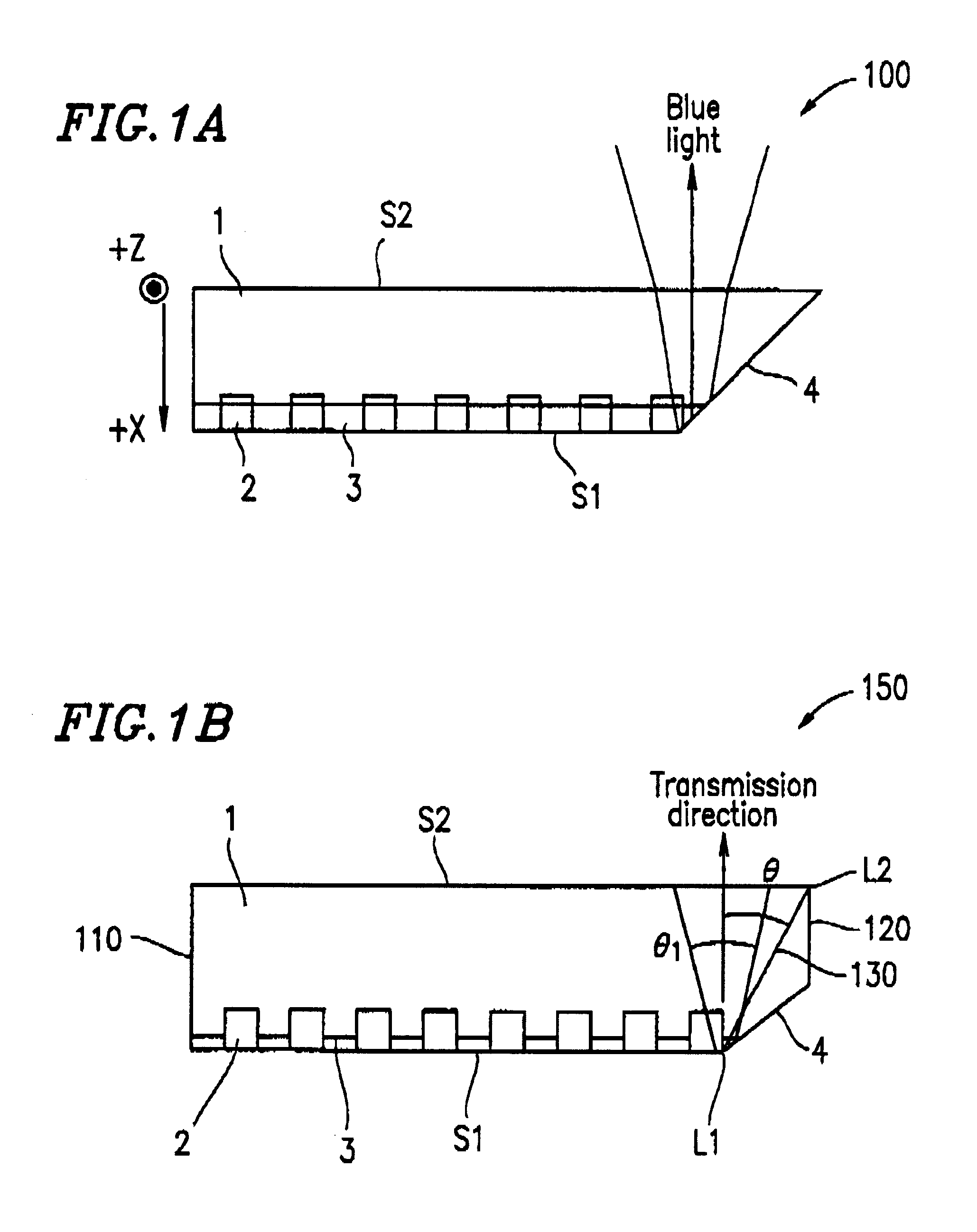
In Example 2, an optical waveguide device has a light-incoming facet and another facet which is inclined with respect to the optical waveguide. A guided light in the optical waveguide is totally reflected off the inclined facet so that the guided light is output through a surface S1 of a substrate on which the optical waveguide is provided.

FIG. 5 is a perspective view schematically showing a structure of a QPM-SHG optical waveguide device 500 according to Example 2 of the present invention. The QPM-SHG optical waveguide device 500 includes a periodic polarization inversion region 16 and a proton exchange waveguide 17 which are provided on a surface S1 of an Mg-doped LiNbO.sub.3 substrate 15. A facet 18 is provided on a side of the optical waveguide 3 opposite a light-incoming side. The facet 18 is inclined with respect to the optical waveguide 3.

The optical waveguide device 500 is fabricated in the following way. An Mg-doped LiNbO.sub.3 substrate 15 having a thickness of about 0.5 m...

example 3

As described above, when an inclined facet having a total reflection angle is provided at an end of an optical waveguide of an optical waveguide device, a guided light is effectively output from the optical waveguide device. Further, when the optical waveguide device is integrated with a semiconductor laser into a light source module, the light source module can be downsized and light emitted from the light source module is stable. Still further, returning light from a facet to the semiconductor laser can be reduced. However, optical polishing is required for formation of the inclined facet having a total reflection angle at the end of the optical waveguide. This poses a problem with cost reduction when such a device is produced in a large quantity. Therefore, in Example 3, a configuration of an optical waveguide device applicable to a wafer process easily adapted to mass production is proposed.

FIG. 8 is a perspective view schematically showing a configuration of an optical waveguid...

example 4

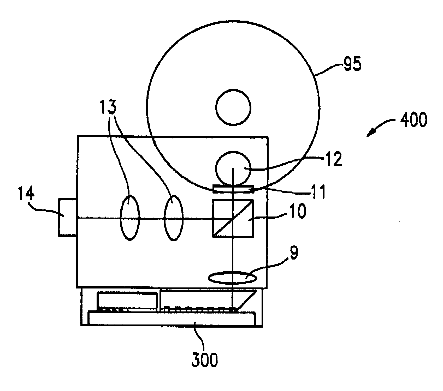
In Example 4, a coherent light source including an optical waveguide device and a semiconductor laser, an integrated unit including the coherent light source and a photodetector which are integrated with the same submount, and an optical pickup including the integrated unit will be described.

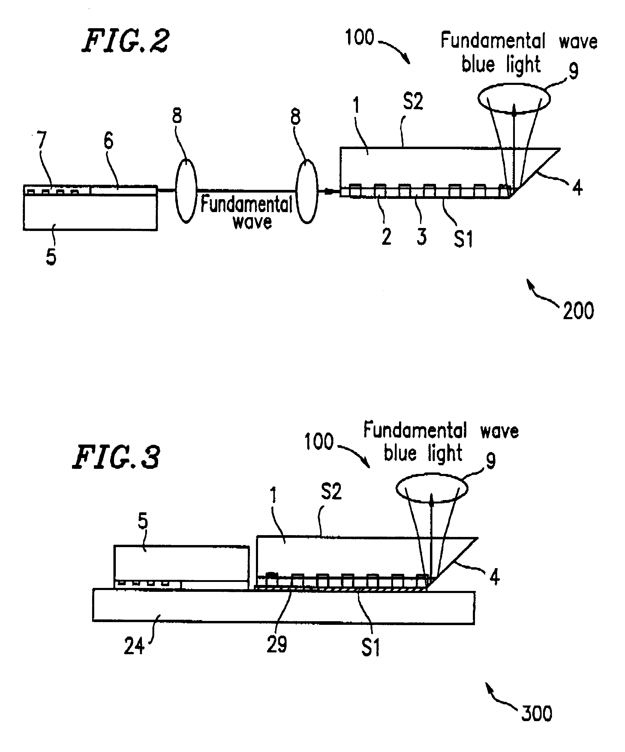
FIG. 12 is a perspective view schematically showing a structure of an optical system of an optical pickup 1200 for optical disks according to Example 4 of the present invention. The optical pickup 1200 includes an integrated unit, and a hologram 53 and an objective lens 53a as a focusing optical system. The integrated unit includes a light source module and photodetectors which are provided on the same submount 55. The light source module includes an optical waveguide device 50 (QPM-SHG device) and a tunable DBR semiconductor laser 56. The optical waveguide device 50 is an optical waveguide device of Example 1 shown in FIG. 1 in which light is output through the substrate surface S2 opposite the...


PUM


Abstract

An optical waveguide device comprises a substrate having first and second surfaces, and an optical waveguide provided on the first surface of the substrate, having a light-incoming facet and a facet inclined with respect to the optical waveguide. Guided light incident to the optical waveguide through the light-incoming facet is totally reflected off the inclined facet, and the guided light is transmitted through the first or second surface of the substrate.

Description

1. Field of the InventionThe present invention relates to an optical waveguide device and a coherent light source for use in a field such as optical information processing or optical communication. The present invention also relates to an integrated unit and an optical pickup device including the optical waveguide device or the coherent light source.2. Description of the Related ArtIn the optical information processing field, a small-sized light source for emitting light having a short wavelength is required for achieving high-density optical disks and high-definition displays. There are know techniques for generating light having a short wavelength. An example of such a technique is a second harmonic generation (hereinafter referred to as "SHG") technique using a semiconductor device and an optical waveguide wavelength conversion (Yamamoto et al., Optics Letters Vol. 16, No. 15, 1156 (1991)) device using quasi phase matching (hereinafter referred to as "QPM").FIG. 20 is a diagram s...

Claims


Application Information

Patent Timeline
Patent Type & Authority Patents(United States)
IPC IPC(8): G02B6/42G02B6/126G02B6/12
CPCG02B6/126G02B6/4214G02B2006/1204
Inventor KITAOKA, YASUOKASAZUMI, KENICHIMIZUUCHI, KIMINORIYAMAMOTO, KAZUHISA
Owner PANASONIC CORP
Why Eureka
Try Eureka