Semiconductor device and method of manufacture thereof

a semiconductor and semiconductor technology, applied in the direction of semiconductor devices, electrical devices, transistors, etc., can solve the problems of unstable etching, difficult to produce required ldd structures or offset gate structures, and inability to maintain a screen display for a set tim

Inactive Publication Date: 2003-01-14
SEMICON ENERGY LAB CO LTD
View PDF47 Cites 78 Cited by
  • Summary
  • Abstract
  • Description
  • Claims
  • Application Information

AI Technical Summary

Problems solved by technology

If the value of this off current is large, the charge held for a pixel falls, and it becomes impossible to maintain a screen display for a set time.
When, however, the active layer is constituted by a silicon film possessing a polycrystalline or a microcrystalline structure, migration of carriers (charges) via the crystal grain boundaries occurs, and this is the cause of off current.
However, in the case of TFTs, unlike the case with known semiconductor integrated circuit technology, there are still many problems that need to be solved, and there is the problem that it is difficult to produce required LDD structures or offset gate structures.
In particular, when it is attempted to form a TFT on an insulating substrate such as a glass substrate, etc., there is the problem that, since the substrate becomes electrostatically charged, reactive ion anisotropic etching fails to function properly and etching therefore becomes unstable, and there is, for example, the problem that it is difficult to form fine patterns with good control.
There also exist amorphous silicon TFTs using amorphous silicon for the active layer, but the mobility in them is low, being 5 cm.sup.2 /Vs, normally about 1 cm.sup.2 /Vs, and considerations of operating speed, and also consideration of the fact that they do not permit production of P-channel TFTs mean that there are considerable restrictions on their use.
The above method directly follows the procedure of a conventional LDD manufacturing process for semiconductor integrated circuits, and it comprises a stage which, if unmodified, is difficult to implement in manufacture of a TFT on a glass substrate, and stages which are undesirable in terms of productivity.
The diff

Method used


Image

  • Semiconductor device and method of manufacture thereof
  • Semiconductor device and method of manufacture thereof
  • Semiconductor device and method of manufacture thereof

Examples


example 2

This example is shown in FIG. 4, and it is one in which, using the invention, an N-channel TFT possessing an overlap LDD and an N-channel TFT that does not possess such an LDD are formed on one and the same substrate.

First, similarly to Example 1, a silicon oxide film was formed to 3000 .ANG. on a substrate 401 (Corning 7059) by a plasma CVD process to constitute a base oxide film 402. Then, an amorphous silicon film for forming an active layer was formed to 500 .ANG. by a plasma CVD process. After that, crystallization was effected by leaving this material in a reducing atmosphere at 550-600.degree. C. for 8-24 hours. There is no objection if a small amount of a catalyst element such as nickel, etc. for promoting crystallization is added at this time. (FIG. 4(A))

Next, the resulting crystalline silicon film 403 was patterned to define silicon films 404 and 405 in the form of islands. These island-shaped silicon films constituted TFT active layers. Then, a 800 .ANG. thick silicon oxi...

example 3

This example is shown in FIG. 5, and it is one in which, using the invention, a complementary circuit consisting of an N-channel TFT possessing a lightly doped drain (LDD) and a P-channel TFT that does not possess an LDD is formed.

First, similarly to Example 1, a silicon oxide film was formed to 3000 .ANG. on a substrate 501 (Corning 7059) by a plasma CVD process to constitute a base oxide film 502. Then, an amorphous silicon film for forming an active layer was formed to 500 .ANG. by plasma CVD process. After that, crystallization was effected by leaving this material in a reducing atmosphere at 550-600.degree. C. for 8-24 hours. There is no objection if a small amount of a catalyst element such as nickel, etc. for promoting crystallization is added at this time. (FIG. 5(A))

Next, the crystalline silicon film 503 was patterned, and silicon films 504 and 505 in the form of islands were defined. These island-shaped silicon films constituted TFT active layers. Then, a 800 .ANG. thick s...

example 4

This example is shown in FIG. 6, and it is one which relates to a monolithic active matrix circuit. In this example, a complementary circuit which was produced by the invention and was constituted by an N-channel TFT and a P-channel TFT possessing lightly doped drain (LDD) regions was used as a drive circuit, and a P-channel TFT that did not possess an LDD was used as a matrix circuit switching element.

First, similarly to Example 1, a silicon oxide film was formed to a thickness of 2000 .ANG. on a substrate 601 (Corning 7059) by a plasma CVD process to constitute a base oxide film 602. Then an amorphous silicon film for constituting an active layer was formed by a plasma CVD process to a thickness of 500 .ANG.. After that, crystallization was effected by leaving the material in a reducing atmosphere at 550-600.degree. C. for 8-24 hours.

Next, the amorphous silicon film was patterned to define silicon films in the form of islands. These island-shaped silicon films constituted TFT acti...


PUM


Abstract

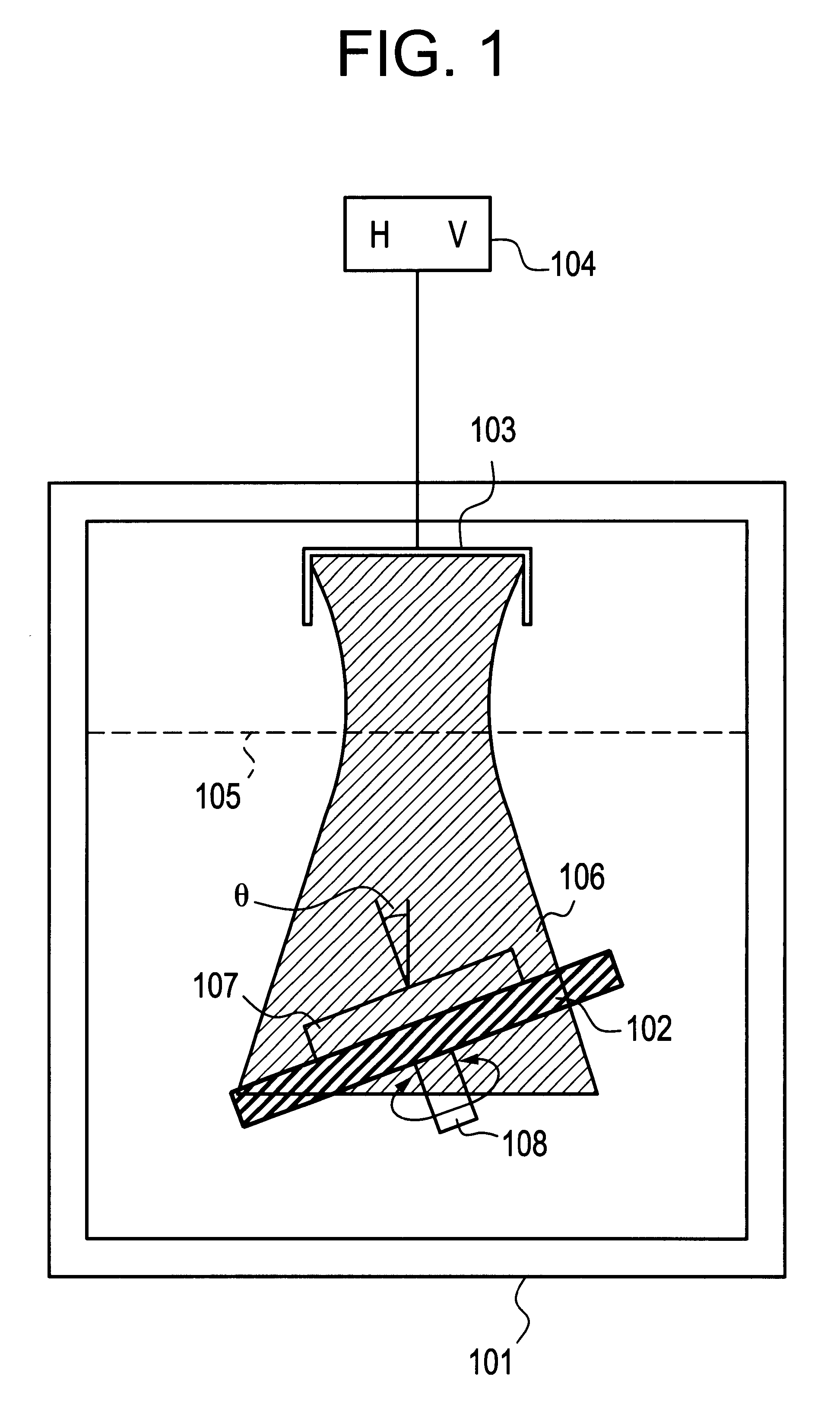
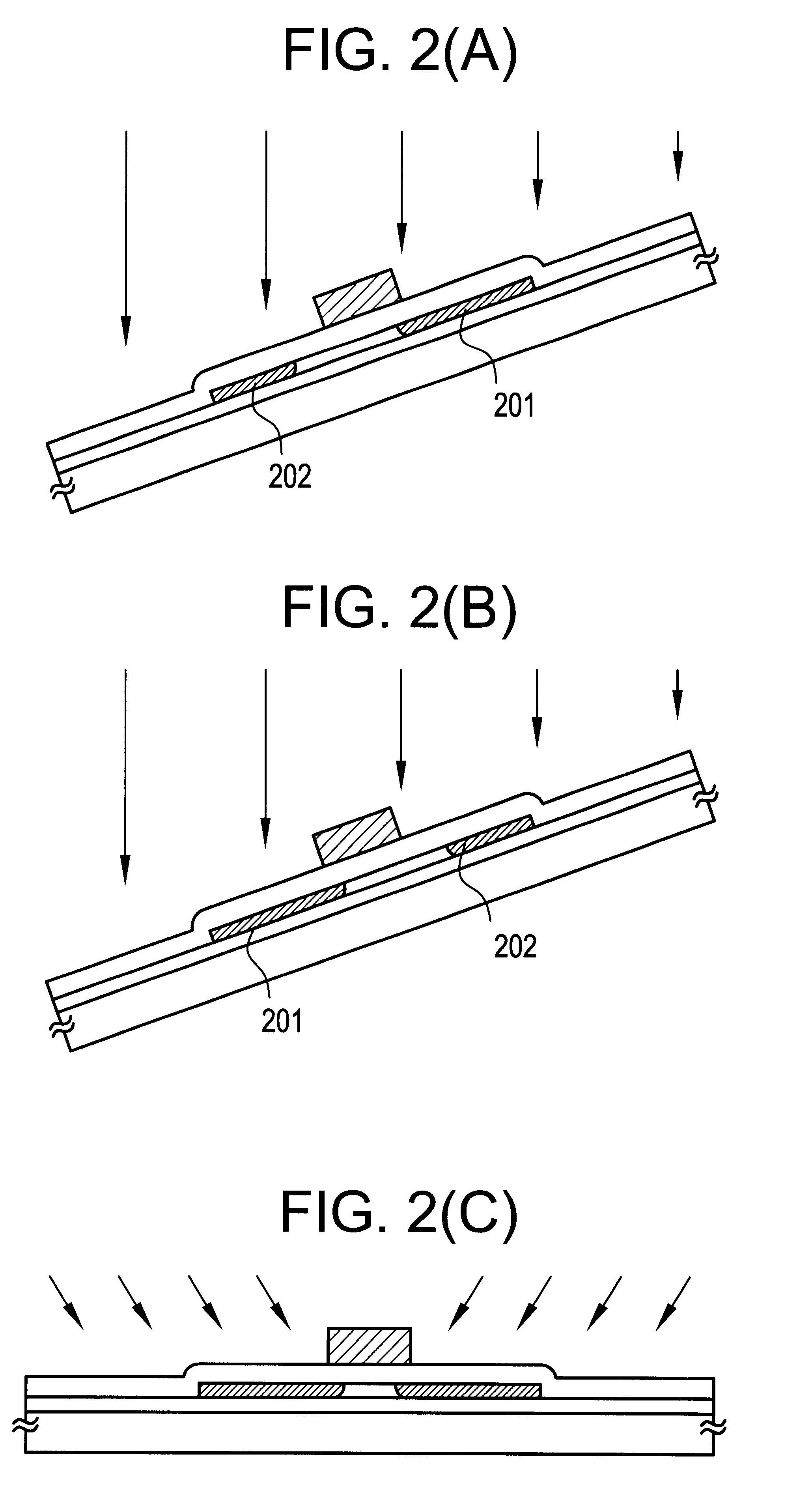
There is provided a method by which lightly doped drain (LDD) regions can be formed easily and at good yields in source/drain regions in thin film transistors possessing gate electrodes covered with an oxide covering. A lightly doped drain (LDD) region is formed by introducing an impurity into an island-shaped silicon film in a self-aligning manner, with a gate electrode serving as a mask. First, low-concentration impurity regions are formed in the island-shaped silicon film by using rotation-tilt ion implantation to effect ion doping from an oblique direction relative to the substrate. Low-concentration impurity regions are also formed below the gate electrode at this time. After that, an impurity at a high concentration is introduced normally to the substrate, so forming high-concentration impurity regions. In the above process, a low-concentration impurity region remains below the gate electrode and constitutes a lightly doped drain region.

Description

1. Field of the InventionThe present invention relates to a method of manufacturing a semiconductor device possessing a lightly doped drain (LDD) region. More particularly, the invention relates to a method of manufacturing a thin film transistor (TFT) possessing a gate electrode which is covered by an oxide film.The invention further relates to a method of forming an insulated gate type semiconductor device which is formed on an insulating surface and possesses a silicon active layer in the form of a thin film and of forming an integrated circuit in which a large number of these devices are formed. The semi-conductor devices of the invention can be used as thin film transistors or integrated circuits of such transistors in the drive circuits of active matrices such as liquid crystal displays, etc. or image sensors, etc. or in SOI integrated circuits and conventional integrated circuits (microprocessors, microcontrollers, microcomputers and semiconductor memories, etc.). In the inve...

Claims


Application Information

Patent Timeline
IPC IPC(8): H01L21/70H01L27/12H01L29/786H01L21/336H01L29/66H01L21/02H01L21/84H01L21/77
CPCH01L27/1214H01L29/78627H01L29/78621H01L29/66757H01L27/127
Inventor ZHANG, HONGYONGTAKEMURA, YASUHIKOKONUMA, TOSHIMITSUOHNUMA, HIDETOYAMAGUCHI, NAOAKISUZAWA, HIDEOMIUOCHI, HIDEKI
Owner SEMICON ENERGY LAB CO LTD
Why Eureka
Try Eureka