Method for forming insulating film and for manufacturing integrated circuit
- Summary
- Abstract
- Description
- Claims
- Application Information
AI Technical Summary
Benefits of technology
Problems solved by technology
Method used
Image

Examples
first embodiment
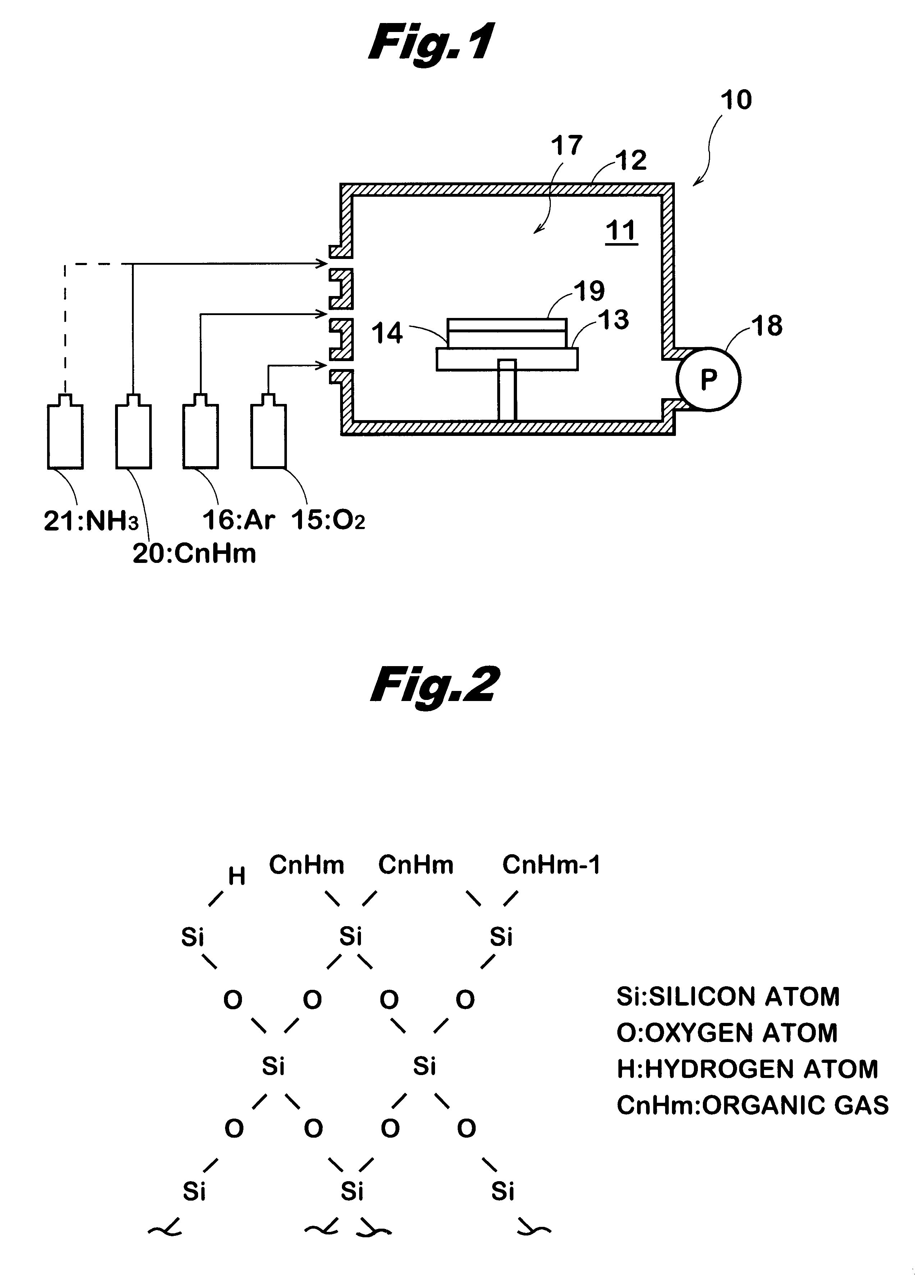
FIG. 1 is a schematic block diagram showing an apparatus to perform a method for forming an insulating film of the present invention.
The insulating film forming apparatus 10 of the first embodiment of the present invention is provided with a housing 12 defining a reaction chamber 11 and a sample stage 13 placed in the housing 12. On the sample gate 13 is held, for example, a silicon crystal substrate 14 with its surface facing upward so that the silicon dioxide film serving as the insulating film grows.
In order to allow the silicon dioxide film having a predetermined thickness to grow on the silicon crystal substrate 14, an inside of the reaction chamber 11 is kept under an atmosphere of ozone, in the same manner as disclosed in the conventional method. Moreover, to provide such the atmosphere in the inside of the reaction chamber 11, oxygen fed from an oxygen source 15 and inert gas such as argon fed from an inert gas source 16 connected to one end of the reaction chamber 11 are su...
second embodiment
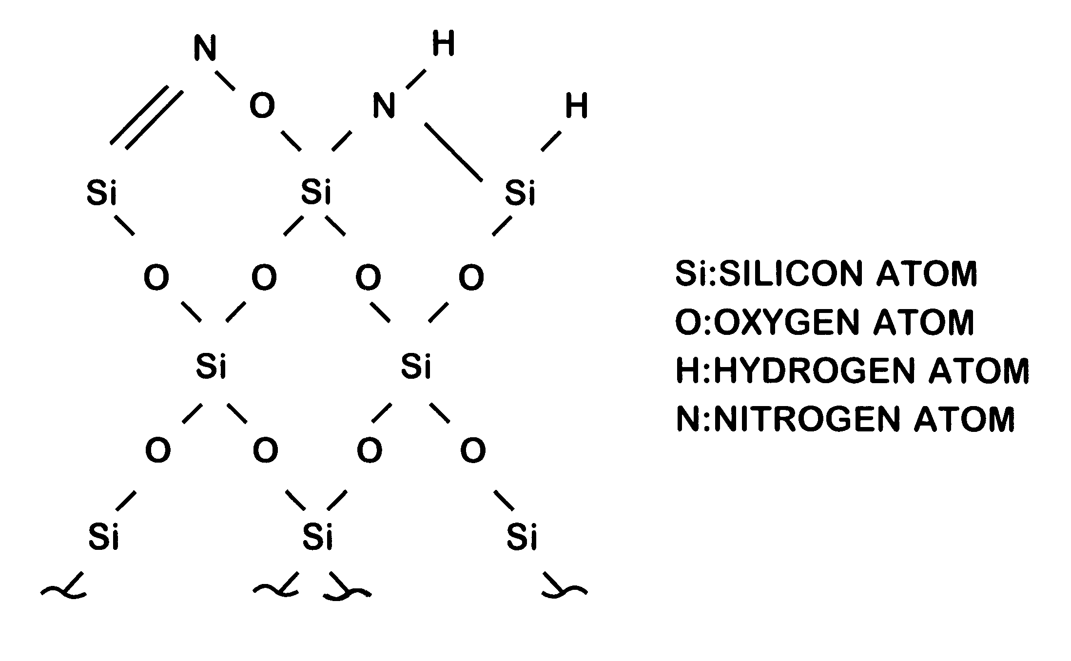
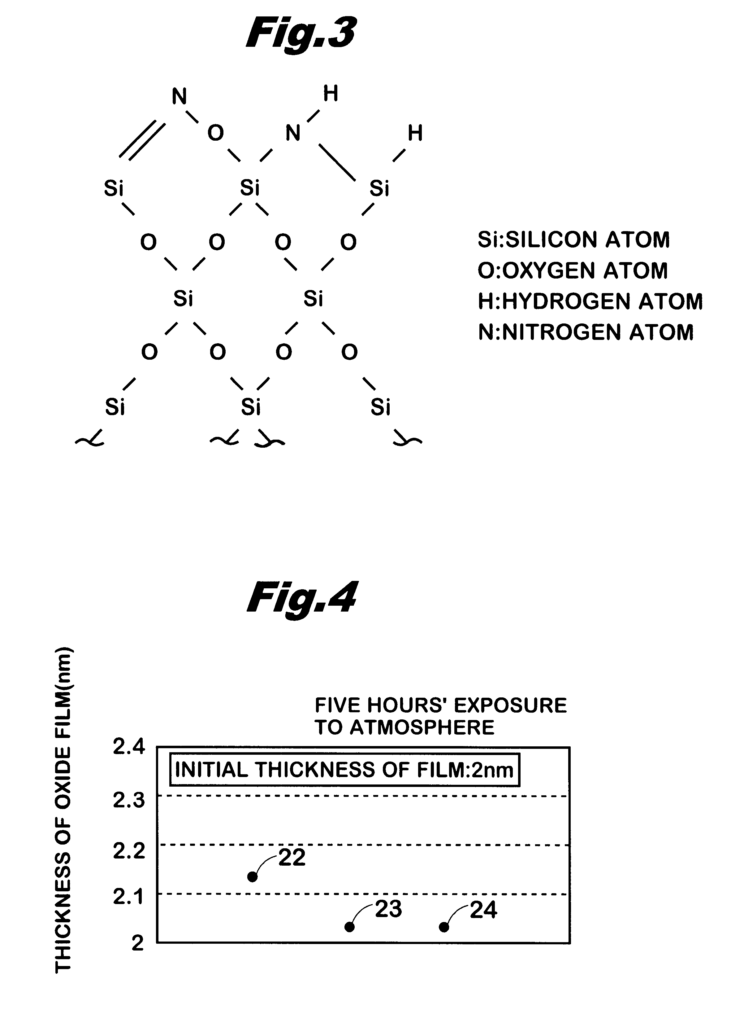
In the above first embodiment, the organic gas is adsorbed on the surface of the silicon dioxide layer 19 or the growth of the silicon dioxide layer 19 is terminated by using the organic gas. However, in a second embodiment, by causing dangling bonds of the silicon atom existing on the surface of the silicon dioxide layer 19 to bind to nitrogen atoms, the bonding of the silicon atom is terminated to inhibit the growth of the silicon dioxide layer 19.
In the second embodiment, in order to cause the dangling bonds of the silicon atoms existing on the surface of the silicon dioxide layer 19 to bind to the nitrogen atoms to inhibit the growth of the silicon dioxide layer 19, instead of the organic gas source 20 shown in FIG. 1, an ammonia gas source 21 is provided. After the silicon dioxide layer 19 having a predetermined thickness has been allowed to grow on the silicon crystal substrate 14 in the same manner as in the first embodiment, in order to prevent the reaction of ammonia gas wi...
PUM
 Abstract
Description
Claims
Application Information