EL device with insulating layer of a bromide or iodide

a thin film, bromide or iodide technology, applied in the direction of discharge tube/lamp details, luminescent screen, discharge tube/lamp details, etc., can solve the problems of poor electron injection efficiency, difficult to obtain stable properties of cathodes, and unstable properties

Inactive Publication Date: 2003-02-25
SHARP KK
View PDF8 Cites 30 Cited by
  • Summary
  • Abstract
  • Description
  • Claims
  • Application Information

AI Technical Summary

Problems solved by technology

However, according to (1), (2) and (3), since Ca, Mg and Li used in cathodes react with moisture to produce hydroxides, there arises a problem in stability.
In addition, according to (3), it is difficult to produce mixture electrodes with maintaining a constant ratio of the two metals, and therefore, it is hard to obtain cathodes having stable properties.
As for (4) and (5), there is a problem in that the electron injection efficiency is poorer compared with the other three.
However, even though such a cathode composed of a metal and an insulator of a fluoride is used for an organic EL device, sufficient injection of electrons into the organic layers has not been achieved yet.
If the thickness is too large, the internal resistance of the device rises and a larger voltage is required to be applied for obtaining a given output.
As a result, the efficiency declines.
On the other hand, if the thickness is too small, pinholes or the like are generated, and a sufficient luminance cannot be obtained from emitted light even if an electric field is applied.

Method used


Image

  • EL device with insulating layer of a bromide or iodide
  • EL device with insulating layer of a bromide or iodide
  • EL device with insulating layer of a bromide or iodide

Examples


embodiment 3

First, ITO films were formed to a thickness of 200 nm on glass substrates of 50 mm square by sputtering and then patterned to have stripes of 2 mm width. After water washing, the resulting substrates were supersonically washed in water for 10 minutes, supersonically washed in acetone for 10 minutes, washed with vapor of isopropyl alcohol for 5 minutes and dried in a dryer at 100.degree. C. for an hour.

Next, the resulting substrates were fixed on substrate holders in a resistive heating deposition apparatus. The pressure in the apparatus was then reduced to a vacuum of 1.times.10.sup.-4 Pa.

Afterwards, N,N'-diphenyl-N,N'-bis(1-naphthyl) 1,1-biphenyl-4,4-diamine (hereinafter referred to as NPD) represented by the following formula: ##STR2##

was deposited as hole transporting layers to a thickness of 50 nm at a deposition rate of 0.2 nm / sec.

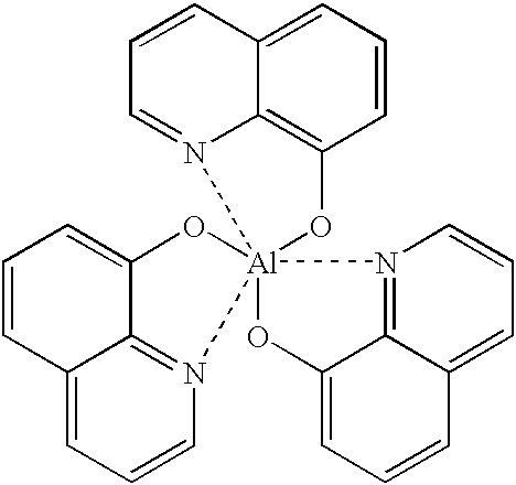
Subsequently, tris(8-hydroxyquinolinate)aluminum (hereinafter referred to as Alq.sub.3) represented by the following formula: ##STR3##

was deposited a...

embodiment 4

Another nine kinds of organic EL devices were produced in the same manner as in Embodiment 3 except that Mg and Ag were co-deposited at deposition rates of 0.4 nm / sec. and 0.04 nm / sec., respectively, to a thickness of 200 nm as cathodes instead of aluminum.

embodiment 5

First, ITO films were formed to a thickness of 200 nm on glass substrates of 50 mm square by sputtering and then patterned to have stripes of 2 mm width. After water washing, the resulting substrates were supersonically washed in water for 10 minutes, supersonically washed in acetone for 10 minutes, washed with vapor of isopropyl alcohol for 5 minutes and dried in a dryer at 100.degree. C. for an hour.

Next, the resulting substrates were fixed on substrate holders in a resistive heating deposition apparatus. The pressure in the apparatus was then reduced to a vacuum of 1.times.10.sup.-4 Pa.

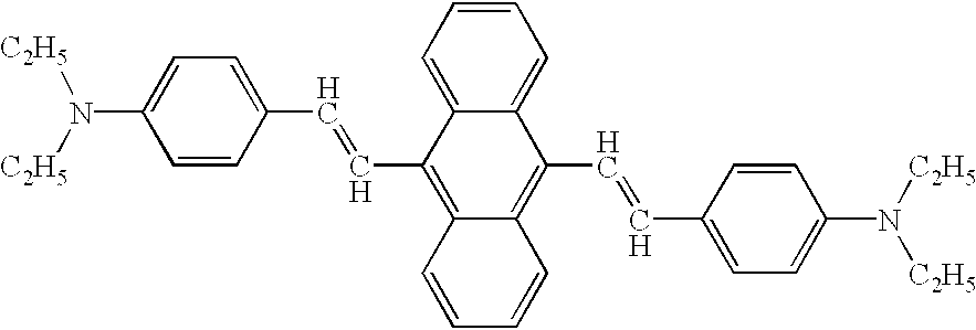
Afterwards, 1,1,4,4,-tetraphenyl-1,3-butadiene (hereinafter referred to as TPB) represented by the following formula: ##STR4##

was deposited as light emitting layers to a thickness of 50 nm at a deposition rate of 0.2 nm / sec.

Subsequently, 2,(4-t-butylphenyl)-5-(4-biphenylyl)-1,3,4-oxazole (hereinafter referred to as tBu-PBD ) represented by the following formula: ##STR5##

was deposited to a thickness...


PUM

PropertyMeasurementUnit
thicknessaaaaaaaaaa
work functionaaaaaaaaaa

Abstract

An organic electroluminescent device having: a pair of an anode and cathode, a single-layered or multi-layered film therebetween containing an organic luminescent material and an insulating film of a chloride, a bromide or an iodide between the cathode and the single-layered or multi-layered film, the device being adapted to emit light by application of voltage or current across the pair of electrodes.

Description

This application is related to Japanese Patent Application No. HEI 11(1999)-070299 filed on Mar. 16, 1999, whose priority is claimed under 35 USC .sctn. 119, the disclosure of which is incorporated by reference in its entirety.1. Field of the InventionThe present invention relates to an organic electroluminescent (hereinafter referred to as EL) device. More particularly, the invention relates to an organic thin-film EL device which can convert electric energy directly to luminous energy when an electric field is applied to its light emitting layer comprised of an organic luminescent substance. The device is usable for a flat light source and a display device.2. Description of Related ArtWith advances of information technology, there has been an increasing need for full color flat panel displays as thinner, less power-consuming and more lightweight display devices than CRTs.Known as such displays are liquid crystal displays (LCDs) which are not self-luminous, and plasma displays (PDP...

Claims


Application Information

Patent Timeline
Patent Type & Authority Patents(United States)
IPC IPC(8): H01L51/50H01L51/52H05B33/02H05B33/12H05B33/14H05B33/22
CPCH01L51/5092H01L51/5221H10K50/171H10K50/82
Inventor FUJITA, YOSHIMASA
Owner SHARP KK
Why Eureka
Try Eureka