Multilayer contact electrode for compound semiconductors and production method thereof

Inactive Publication Date: 2003-03-11
VISHAY SEMICON
View PDF15 Cites 13 Cited by
  • Summary
  • Abstract
  • Description
  • Claims
  • Application Information

AI Technical Summary

Benefits of technology

to provide a method for the production of multilayer contact electrodes applied to a p-type semiconductor layer of a semiconductor body made of a III / V-compound semiconductor in such a way that a simply structured contact electrode is assured and that diffusion problems are avoided without the need for a barrier layer;
to construct the contact electrode in such a way that the contacting or bonding with a bonding wire is assured without any problems and so that a reliable bond results;
to provide a multilayer contact electrode that is, subsequently to its manufacture, easily structured or shaped for the intended purpose of wire bonding.
The present method of manufacturing the multilayer contact electrode is simple in its nature and therefore the electrode is easily produced in economical ways because the multilayer or the two layers are made of the same metal of which only the first or inner layer is tempered. Furthermore, the need for a diffusion barrier layer has been avoided, which also is an economical advantage.
Another advantage of the invention is seen in that the present contact electrode assures a reliable bonding with a bonding wire. Moreover, the present semiconductor components equipped with the present contact electrode are particularly suitable for the manufacture of diodes for emitting infrared radiation. Such diodes are especially used of the wireless transmission of data or in various types of sensors.

Problems solved by technology

The use of gold alloys for this purpose has the disadvantage that during the tempering of the contact electrode 16 contaminations can diffuse into the gold alloy.
Such oxidization causes substantial problems during wire bonding because the wire bonds do not stick to the oxide layers, whereby many wire connections are faulty and become rejects.
Further disadvantages of gold alloys for the above purpose reside in the fact that the multilayer contact electrode 16 can be structured only in several process steps, thereby using different etching solutions.
Such etching procedures, due to their nature, lead to undesirable and hard to control under etching, which means etching of lower layers in the multilayer contact electrode.
The thermal treatment of the aluminum makes the aluminum brittle and on the surface of the contact a film is formed which contains gallium oxide and aluminum oxide as well as hydroxide, whereby the attachment of a bonding wire is again impaired and difficult.
However, the formation of intermetallic phases lead to a problem of reliability during operation of semiconductor components provided with such gold alloy and pure aluminum combinations.
The manufacture and subsequent structuring or shaping of a multi-layer contact electrode 16 made of several metals is relatively expensive, particularly due to the need for a diffusion barrier 16B.
The production of such a layer is involved and time consuming so that cost increases are unavoidable.

Method used


Image

  • Multilayer contact electrode for compound semiconductors and production method thereof
  • Multilayer contact electrode for compound semiconductors and production method thereof
  • Multilayer contact electrode for compound semiconductors and production method thereof

Examples


Embodiment Construction

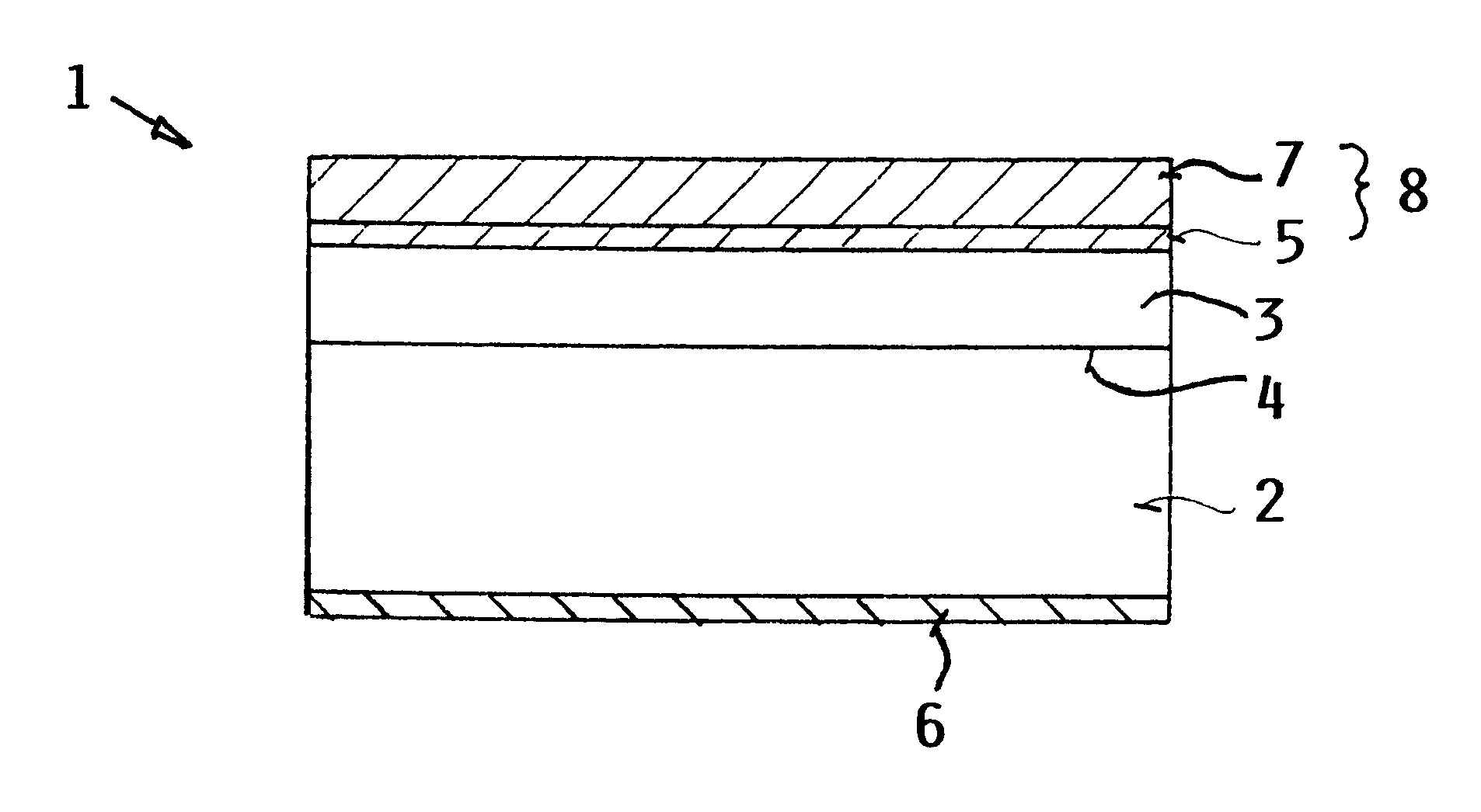
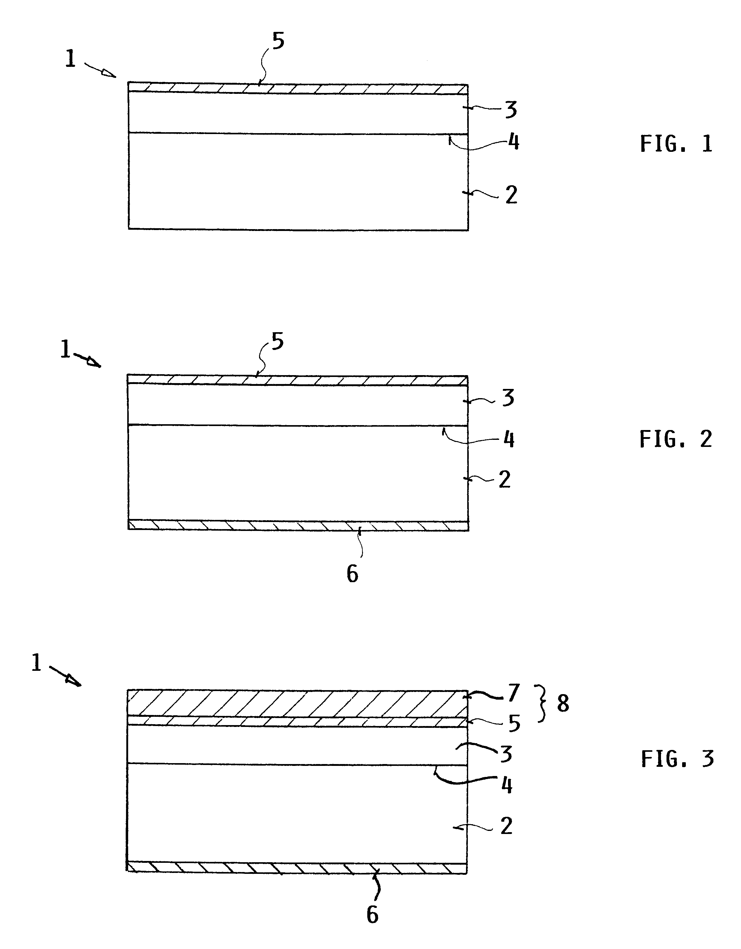
FIG. 1 shows the layer sequence of a semiconductor body or chip 1 for an infrared diode made of a III / V-mixed crystal or compound semiconductor such as gallium arsenide or gallium aluminum arsenide. The chip 1 has an n-type semiconductor layer 2 and a p-type semiconductor layer 3 which constitutes the radiation emitting surface of the chip 1. A p-n junction 4 is present between the n-type layer 2 and the p-type layer 3. Both semiconductor layers 2 and 3 may be made individually of several different layers. For example, the n-type semiconductor layer 2 may comprise an n-type gallium arsenide substrate and an n-type epitaxial semiconductor layer.

The present method is performed as follows. A first metallized or metal layer 5 of aluminum having a thickness within the range of about 0.01 .mu.m to about 0.5 .mu.m is applied to the p-type top surface of the semiconductor layer 3 at a temperature above 350.degree. C. This application may, for example, be made by vapor deposition or cathode ...


PUM


Abstract

A multilayer contact electrode for connecting a bonding wire to a p-type surface of a III / V-compound semiconductor is formed by a first metallizing step followed by a tempering step. Then, a second metallized layer of the same metal as the first metal layer is formed on the first layer but tempering of the second layer is avoided. A reliable bonding of a bonding wire to the non-tempered contact electrode is assured. The contact electrode includes a first inner metallized layer that is tempered and covered by a second nontempered metallized layer of the same metal as the first layer.

Description

The invention relates to a method for producing multilayer contact electrodes for compound semiconductors. The invention also relates to such a multilayer contact electrode and to compound semiconductors equipped with such a multilayer contact electrode.BACKGROUND INFORMATIONJapanese Patent Abstracts Publication JP 11-054843 a, JPO, 1999 discloses a method for producing multilayer contact electrodes for the p-type semiconductor layer of a semiconductor body made of a III / V-compound semiconductor. In the known method first a metallized layer is applied on the p-type semiconductor layer. The metallized layer is then exposed to a heat treatment or tempering at a temperature of 400.degree. C. Thereafter, further layers consisting of different metals including a barrier layer 13 of titanium are applied to the first metallized layer.Japanese Patent Abstract Publications JP 62-35587 A, E-522, 1987, Vol. 11, No. 212 describes a multilayer contact electrode for a light emitting semiconductor...

Claims


Application Information

Patent Timeline
IPC IPC(8): H01L21/02H01L29/45H01L21/285H01L29/40H01L33/00H01L33/30H01L33/40
CPCH01L21/28575H01L33/40H01L29/452H01L33/30
Inventor GERNER, JOCHEN
Owner VISHAY SEMICON
Why Eureka
Try Eureka